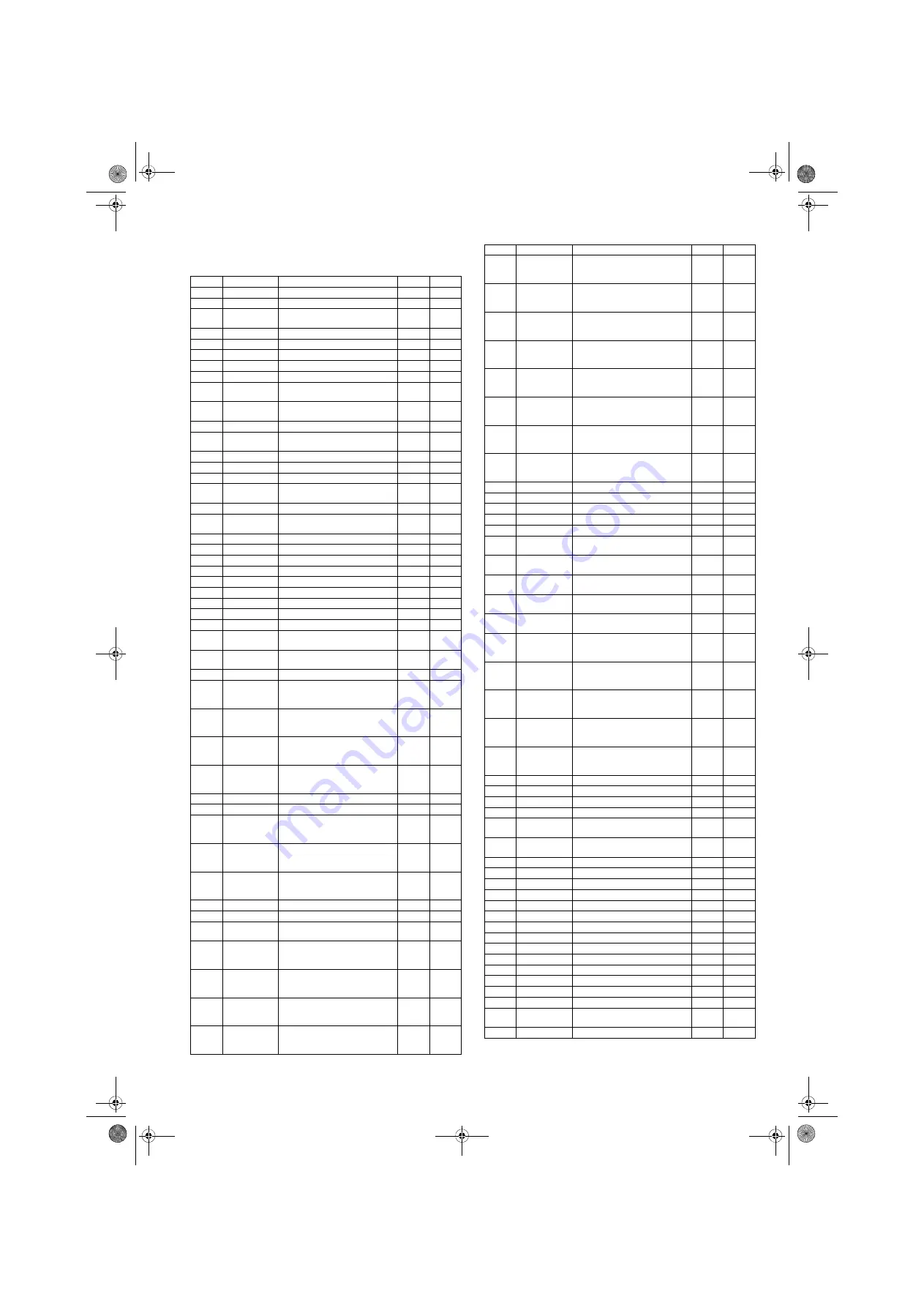
6
IC800:C5ZBZ0000148
Pin No.
Port
Description
I/O
CD(V)
1
EFMIN
RF signal input.
AI
1.61
2
RFOUT
RF signal output.
AO
1.56
3
LPF
RF signal DC level detection LPF
connection.
AO
1.55
4
PHLPF
Defect detection LPF connection.
AO
2.20
5
AIN
A signal input.
AI
1.63
6
CIN
C signal input.
AI
1.63
7
BIN
B signal input.
AI
1.62
8
DIN
D signal input.
AI
1.66
9
SLCISET
SLCO output current setting resis-
tor connection.
AI
1.69
10
RFMON
IC internal analog signal monitor
1.
AO
1.54
11
VREF
VREF voltage output.
AO
1.57
12
JITTC
Jitter detection capacitor connec-
tion.
AO
0.68
13
EIN
E signal input.
AI
1.64
14
FIN
F signal input.
AI
1.64
15
TE
TE signal output.
AO
1.60
16
TEIN
TE signal input used for TES sig-
nal generation.
AI
1.57
17
LDD
Laser power control signal output.
AO
2.18
18
LDS
Laser power detection signal
input.
AI
0
19
AVSS
Analog system ground.
-
0
20
AVDD
Analog system power supply.
-
3.11
21
FDO
Focus control signal output.
AO
1.44
22
TDO
Tracking control signal output.
AO
1.69
23
SLDO
Sled control signal output.
AO
1.80
24
SPDO
Spindle control signal output.
AO
1.64
25
VVDD1
EFMPLL power supply.
-
3.11
26
PDOUT1
EFMPLL charge pump output 1.
AO
1.20
27
PDOUT0
EFMPLL charge pump output 0.
AO
1.19
28
PCNCNT
EFMPLL charge pump control
voltage input.
AI
3.11
29
PCKIST
EFMPLL charge pump current
setting resistor connection.
AI
1.12
30
VVSS1
EFMPLL ground.
-
0
31
GP10
General purpose I/O port with pull
down resistor. UART 1 data trans-
mit.
I/O
2.97
32
GP11
General purpose I/O port with pull
down resistor. UART 1 data
receive.
I/O
0
33
GP12
General purpose I/O port with pull
down resistor. External interrup-
tion function 2.
I/O
0
34
GP13
General purpose I/O port with pull
down resistor. External interrup-
tion function 3.
I/O
0
35
DVDD
Digital system power supply.
-
3.11
36
DVSS
Digital system ground.
-
0
37
GP43
General purpose I/O port with pull
down resistor. Transmit data out-
put for serial communication 2.
I/O
3.12
38
GP44
General purpose I/O port with pull
down resistor. Receive data input
for serial communication 2.
I/O
3.12
39
GP45
General purpose I/O port with pull
down resistor. Master clock output
for serial communication 2.
I/O
0
40
DVDD
Digital system power supply.
-
3.11
41
DVSS
Digital system ground.
-
0
42
DVDD15
Capacitor connection pin for inter-
nal regulator.
AO
1.61
43
GP50
General purpose I/O port with pull
down resistor. USB over current
detection signal input.
I/O
3.12
44
GP51
General purpose I/O port with pull
down resistor. UART 2 data trans-
mit.
I/O
0
45
GP52
General purpose I/O port with pull
downr resistor. UART 2 data
receive.
I/O
0
46
GP53
General purpose I/O port with pull
down resistor. USB power supply
signal output.
I/O
0
47
GP30
General purpose I/O port with pull
down resistor. External interrup-
tion function 3.
I/O
0
48
GP31
General purpose I/O port with pull
down resistor. Bit clock input/out-
put for Stream data.
I/O
0
49
GP32
General purpose I/O port with pull
down resistor. Data input/output
for Stream data.
I/O
3.11
50
GP33
General purpose I/O port with pull
down resistor. Request flag input/
output for Stream data.
I/O
0
51
GP34
General purpose I/O port with pull
down resistor. Transmit data out-
put for serial communication 3.
I/O
0
52
GP35
General purpose I/O port with pull
down resistor. Master clock output
for serial communication 3.
I/O
0
53
GP36
General purpose I/O port with pull
down resistor. Receive data input
for serial communication 3.
I/O
0
54
GP37
General purpose I/O port with pull
down resistor. Data 2 input/output
for SD memory card.
I/O
0
55
MODE0
LSI mode set pin 0.
I
0
56
MODE1
LSI mode set pin 1.
I
0
57
DVDD
Digital system power supply.
-
3.12
58
DVSS
Digital system ground.
-
0
59
RESB
IC reset input.L-active.
I
4.69
60
SIFCK
Data transmit clock input for serial
communication1.
I
4.67
61
SIFDI
Data input for serial communica-
tion 1.
I/O
4.17
62
SIFDO
Data output for serial communica-
tion 1.
I/O
2.00
63
SIFCE
Enable signal input for serial com-
munication 1.
I/O
2.30
64
BUSYB
System busy signal ooutput.
External interruption function 0.
I/O
2.94
65
GP03
General purpose I/O port with pull
down resistor. Watch dog timer
state monitor output.
I/O
0
66
GP04
General purpose I/O port with pull
down resistor. Master clock output
for serial communication 2.
I/O
3.12
67
GP05
General purpose I/O port with pull
down resistor. Receive data input
for serial communication 2.
I/O
3.12
68
GP06
General purpose I/O port with pull
down resistor. Transmit data out-
put for serial communication 2.
I/O
0
69
GP07
General purpose I/O port with pull
down resistor. UART 1 data
receive.
I/O
0
70
XVDD1
Oscillator power supply.
-
3.12
71
XIN
12MHz oscillator connection.
I
1.58
72
XOUT
12MHz oscillator connection.
O
1.52
73
XVSS1
Oscillator ground.
-
0
74
UDM
USB data input/output. D- signal
connection.
I/O
0
75
UDP
USB data input/output. D+ signal
connection.
I/O
0
76
UVDD
USB power supply.
-
3.11
77
VVDD2
System PLL power supply.
-
3.11
78
VVSS2
System PLL ground.
-
0
79
AFILT
Audio PLL charge pump output.
AO
1.66
80
VVDD3
Audio PLL power supply.
-
3.11
81
MODE2
LSI mode set pin 2.
I
0
82
JTRSTB
JTAG reset input.
I
0
83
JTCK
JTAG clock input.
I
0
84
JTDI
JTAG data input.
I
0
85
JTMS
JTAG mode input.
I
3.12
86
JTDO
JTAG mode output.
O
0
87
JTRTCK
JTAG return clock output.
O
0
88
DVDD
Digital system power supply.
-
3.11
89
DVSS
Digital system ground.
-
0
90
DVDD15
Capacitor connection pin for inter-
nal regulator.
AO
1.62
91
XVSS2
Oscillator ground.
-
0
Pin No.
Port
Description
I/O
CD(V)
cqrxbt490u.book Page 6 Friday, April 6, 2012 9:48 AM
Содержание SiriusXM CQ-RXBT490U
Страница 10: ...10 IC201 C1BA00000493 IC602 C3EBJY000032 cqrxbt490u book Page 10 Friday April 6 2012 9 48 AM ...
Страница 11: ...11 IC400 C1BB00001088 cqrxbt490u book Page 11 Friday April 6 2012 9 48 AM ...
Страница 12: ...12 IC50 C1ZBZ0004389 IC706 C0DBGYY00710 cqrxbt490u book Page 12 Friday April 6 2012 9 48 AM ...
Страница 13: ...13 IC707 C0DBGYY00710 IC180 C0CBCYG00004 cqrxbt490u book Page 13 Friday April 6 2012 9 48 AM ...
Страница 14: ...14 IC701 C0DAZYY00033 cqrxbt490u book Page 14 Friday April 6 2012 9 48 AM ...
Страница 15: ...15 IC803 C1AB00003758 cqrxbt490u book Page 15 Friday April 6 2012 9 48 AM ...
Страница 16: ...16 IC705 C0EBY0001290 cqrxbt490u book Page 16 Friday April 6 2012 9 48 AM ...
Страница 17: ...17 IC902 B3RAB0000091 IC181 C0JBAB000255 cqrxbt490u book Page 17 Friday April 6 2012 9 48 AM ...
Страница 42: ...42 10 5 Packing Parts List 1 2 3 5 6 4 7 11 10 9 8 cqrxbt490u book Page 42 Friday April 6 2012 9 48 AM ...
Страница 50: ...50 2012 03 T cqrxbt490u book Page 50 Friday April 6 2012 9 48 AM ...