


UM11082
All information provided in this document is subject to legal disclaimers.
© NXP B.V. 2018. All rights reserved.
User Manual
Rev. 1.1 — 12 January 2018
6 of 18
NXP Semiconductors
LPC8N04 Development Board
User Manual
3. Getting
Started
The LPC8N04 device flash is pre-programmed with an example application, which scrolls
a message across the LED array on the bottom side of the board and plays a tune through
the micro speaker. The jumpers are positioned for that demonstration by default. This
section describes how to run the demonstration, and how to re-configure the board to start
code development. If using Windows 7 or 8, before powering up the board, you will need
to install device drivers for the VCOM port.
3.1 Installing device drivers (Windows 7 and 8 only)
The firmware for the on-board debug probe and Windows 7/8 driver for the virtual com
(VCOM) port are available from http://nxp.com/demoboard/OM40002 under the Software
and Tools tab (look under “Software” download types). The debug probe firmware is
factory installed so should not normally need updating, but if using Window 7 or 8, you will
need to install the VCOM driver by running the installer program before attempting to use
the board. After downloading and unzipping the package, run the installer program
provided to install the driver (see installation notes included in the package for further
information.)
3.2 Running the out-of-box demo
The LPC8N04 on the Development Board is pre-programmed with a demonstration
program, which designed illustrate the features of the device by working with an
NFC-enabled smartphone running a free App from NXP. For best results, an smart phone
running Android Nougat or later is recommended. The demonstration program (in
conjunction with the App) shows two way communication between a smartphone and the
LPC8N04, passing messages, temperature and tune selection information between the
two devices. Some aspects of the demonstration application can be used without any
power being supplied to the Development Board; these are mentioned in this section
below.
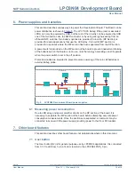
The LPC8N04 supports SWD debug, requiring two I/O pins. Alternatively, these pins can
be used as GPIOs. On the Board these two SWD/GPIO signals are connected to two of
the LED array columns via jumpers P7 and P8. To use the full number of LED columns,
the P8 and P7 jumpers need to be set as shown in
Figure 3
.
On GPIO from the LPC8N04 is shared between a row of the LED array and the speaker,
using a jumper (P9) to select which function is used, as shown in
Figure 3
. If no jumper is
fitted then neither the LED row nor the speaker will be enabled.
On the Target (right) side of the board, there is a power switch. This is to prevent
accidental running down of the battery, when used. The switch should be in the up
position to provide power to the LPC8N04.