


UM11082
All information provided in this document is subject to legal disclaimers.
© NXP B.V. 2018. All rights reserved.
User Manual
Rev. 1.1 — 12 January 2018
3 of 18
NXP Semiconductors
LPC8N04 Development Board
User Manual
1. Introduction
The LPC8N04 Development Board board is developed by NXP to enable evaluation of
and prototyping with the LPC8N04 MCU.
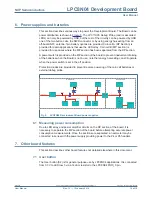
Figure 1
shows each side of LPC8N04
Development Board. The LPC8N04 device, buttons, jumpers and debug probe circuitry
are on the top side (along with the board name). On the bottom side is a 5x7 array of
LEDs, plus a surface mount speaker (LS1).
The LPC8N04 Development Board board includes the following features:
•
Compatible with MCUXpresso IDE and other popular toolchains (incl. IAR and Keil)
•
Detachable, two-section board featuring minimal LPC8N04 system and debug probe /
demo circuitry (LEDs and speaker)
•
LPC8N04 Arm Cortex-M0+ MCU running at up to 8MHz
•
Integrated NFC antenna
•
Dual coin cell battery holders for
•
On-board CMSIS-DAP (debug probe) with VCOM port, based on LPC11U35 MCU
•
Debug connector to allow debug of target LPC8N04 MCU using an external probe
•
LPC8N04 User button
•
LPC8N04 Reset button
•
5x7 LED array for user applications
•
Surface mounted speaker with amplifier
•
Expansion connections with pin-outs compatible with I
2
C Grove and Pmod
connectors for easy connection of sensors
Fig 1.
LPC8N04 Development Board