


UM11082
All information provided in this document is subject to legal disclaimers.
© NXP B.V. 2018. All rights reserved.
User Manual
Rev. 1.1 — 12 January 2018
5 of 18
NXP Semiconductors
LPC8N04 Development Board
User Manual
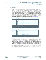
P10
P10 is provided in order to connect a piezo-type speaker (after first
removing the on-board SMD speaker). This jumper is bypassed by R2
(zero ohm resistor) by default.
[7.3]
J1
External debug probe connector. Install P1 when using this header.
[4.1]
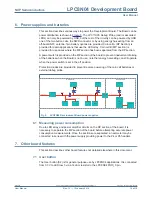
S1
LPC8N04 power on/off switch. When the switch is open the power is
disconnected from the LPC8N04. This switch is provided to prevent
accidental draining of the batteries.
[6]
S2
User button. This resistor is connected to the PIO0_3 pin of the LPC8N04
and can be used in user applications. When S2 is pressed, PIO0_3 is
pulled to ground via a 1k ohm resistor. Note that PIO0_3 also drives row 5
of the LED array.
[7.1]
S3
LPC8N04 reset button. This button resets the LPC8N04 (note that no
other circuitry is reset by this button.
n/a
Table 1.
Jumpers and connectors
Circuit reference
Description
Reference section