


DR
AFT
DR
AFT
DRAFT
DR
D
RAFT
DRAFT
DRA
FT DRAF
D
RAFT DRAFT DRAFT DRAFT DRAFT D
DRAFT
D
RAFT DRA
FT DRAFT DRAFT DRAFT DRA
LPC2917_19_1
© NXP B.V. 2007. All rights reserved.
Preliminary data sheet
Rev. 1.01 — 15 November 2007
38 of 68
NXP Semiconductors
LPC2917/19
ARM9 microcontroller with CAN and LIN
•
Automotive dimmer controller: The flexibility of providing waves of a desired duty
cycle and cycle period allows the PWM to control the amount of power to be
transferred to the load. The PWM functions as a dimmer controller in this application
•
Motor controller: The PWM provides multi-phase outputs, and these outputs can be
controlled to have a certain pattern sequence. In this way the force/torque of the
motor can be adjusted as desired. This makes the PWM function as a motor drive.
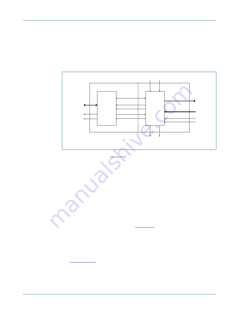
The PWM block diagram in
Figure 10
shows the basic architecture of each PWM. PWM
functionality is split into two major parts, a VPB domain and a PWM domain, both of which
run on clocks derived from the BASE_MSCSS_CLK. This split into two domains affects
behavior from a system-level perspective. The actual PWM and prescale counters are
located in the PWM domain but system control takes place in the VPB domain.
The actual PWM consists of two counters; a 16-bit prescale counter and a 16-bit PWM
counter. The position of the rising and falling edges of the PWM outputs can be
programmed individually. The prescale counter allows high system bus frequencies to be
scaled down to lower PWM periods. Registers are available to capture the PWM counter
values on external events.
Note that in the Modulation and Sampling SubSystem, each PWM has its individual clock
source CLK_MSCSS_PWMx (x runs from 0 to 3). Both the prescale and the timer
counters within each PWM run on this clock CLK_MSCSS_PWMx, and all time references
are related to the period of this clock. See
Section 8.8
for information on generation of
these clocks.
8.7.6.3
Synchronizing the PWM counters
A mechanism is included to synchronize the PWM period to other PWMs by providing a
sync input and a sync output with programmable delay. Several PWMs can be
synchronized using the trans_enable_in/trans_enable_out and sync_in/sync_out ports.
See
Section 8.7.2.1
for details of the connections of the PWM modules within the MSCSS
in the LPC2917/19. PWM 0 can be master over PWM 1; PWM 1 can be master over
PWM 2, etc.
Fig 10. PWM block diagram
PWM
control
&
registers
PWM
Counter,
prescale
counter
&
shadow
registers
VPB system bus
update
Capture data
Config data
IRQ’s
Sync_in
Capture inputs
IRQ capt_match
PWM domain
VPB domain
IRQ pwm
Match outputs
PWM counter value
Transfer_enable_in
Transfer_enable_out
Sync_out
Carier inputs
Trap input