


DR
AFT
DR
AFT
DRAFT
DR
D
RAFT
DRAFT
DRA
FT DRAF
D
RAFT DRAFT DRAFT DRAFT DRAFT D
DRAFT
D
RAFT DRA
FT DRAFT DRAFT DRAFT DRA
LPC2917_19_1
© NXP B.V. 2007. All rights reserved.
Preliminary data sheet
Rev. 1.01 — 15 November 2007
32 of 68
NXP Semiconductors
LPC2917/19
ARM9 microcontroller with CAN and LIN
control. Several other trigger possibilities are provided for the ADCs (external, cascaded
or following a PWM). The capture inputs of both timers can also be used to capture the
start pulse of the ADCs.
The PWMs can be used to generate waveforms in which the frequency, duty cycle and
rising and falling edges can be controlled very precisely. Capture inputs are provided to
measure event phases compared to the main counter. Depending on the applications,
these inputs can be connected to digital sensor motor outputs or digital external signals.
Interrupt signals are generated on several events to closely interact with the CPU.
The ADCs can be used for any application needing accurate digitized data from analog
sources. To support applications like motor control, a mechanism to synchronize several
PWMs and ADCs is available (sync_in and sync_out).
Note that the PWMs run on the PWM clock and the ADCs on the ADC clock, see
Section 8.8.4
.
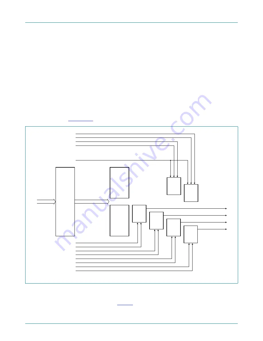
8.7.2.1
Synchronization and trigger features of the MSCSS
The MSCSS contains two internal timers to generate synchronization and carrier pulses
for the ADCs and PWMs.
Figure 8
shows how the timers are connected to the ADC and
PWM modules.
Fig 7.
Modulation and sampling control subsystem block diagram
002aad348
PWM0 MAT[5:0]
PWM1 MAT[5:0]
PWM2 MAT[5:0]
PWM3 MAT[5:0]
ADC
1
3.3 V
ADC
2
3.3 V
PWM
0
MSCSS
TIMER 1
PWM
CONTROL
CARRIERS
MSCSS
TIMER 0
ADC
CONTROL
SYNCS
AHB2VPB
BRIDGE
PWM
1
PWM
2
PWM
3
AHB
system bus
VPB sub system bus
(to all sub blocks)
ADC2 IN[7:0]
ADC2_EXT_START
ADC1 IN[7:0]
ADC1_EXT_START
ADC clock
PWM0 TRAP
PWM0 CAP[2:0]
PWM1 TRAP
PWM1 CAP[2:0]
PWM2 TRAP
PWM2 CAP[2:0]
PWM3 TRAP
PWM3 CAP[2:0]