background image

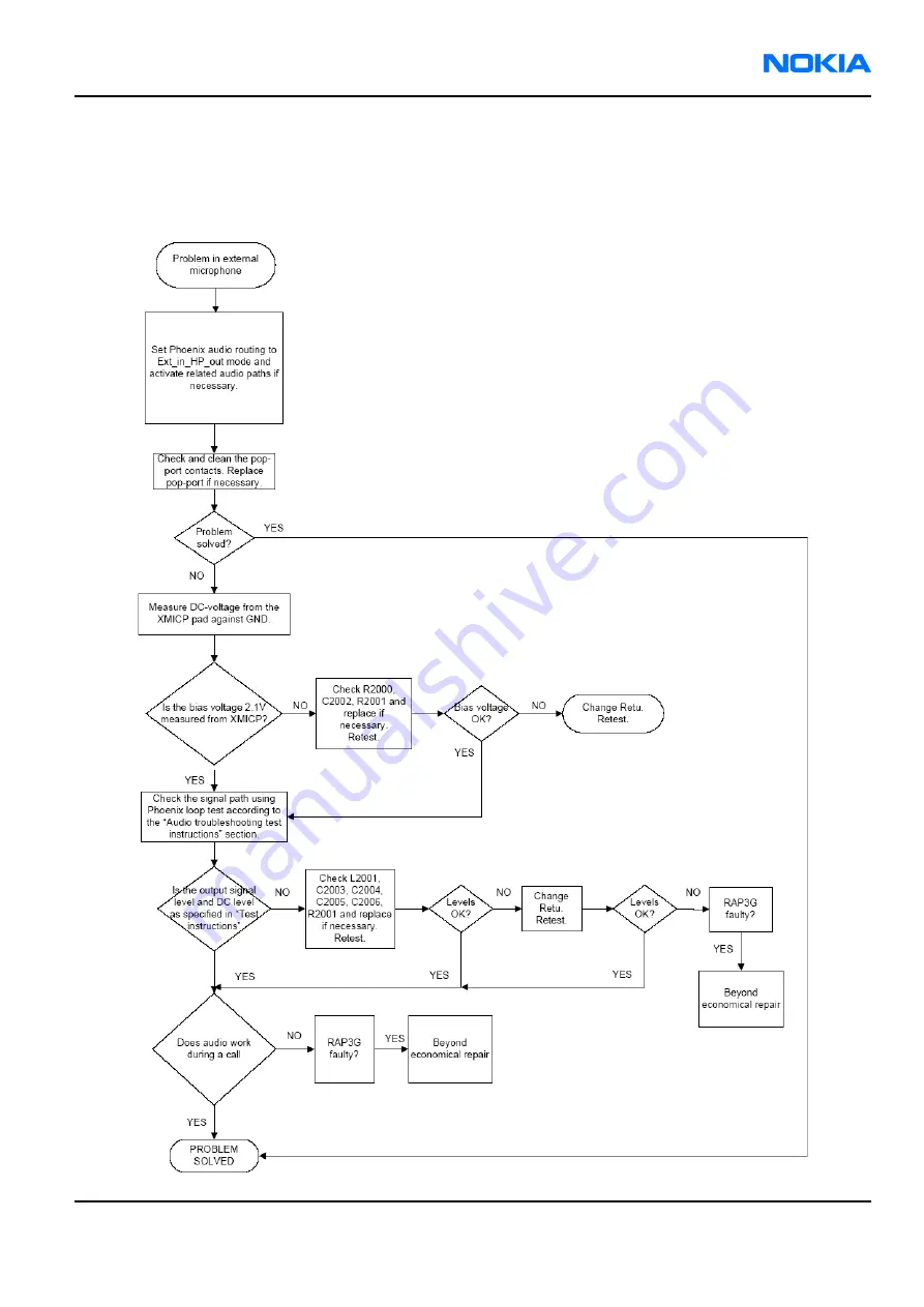
External microphone troubleshooting

Before you begin

Familiarize yourself with the 

Audio troubleshooting test instructions (Page 6–38)

.

RM-42
BB Troubleshooting and Manual Tuning Guide

Nokia Customer Care

9241872 (Issue 1)

Company Confidential

Page 6–47

Copyright ©2005 Nokia. All Rights Reserved.

Содержание RM-42

Страница 1: ...Service Manual RM 42 Nokia N90 Mobile Terminal Part No 9241872 Issue 1 Nokia Customer Care Company Confidential Copyright 2005 Nokia All Rights Reserved ...

Страница 2: ...t Record Sheet Amendment No Date Inserted By Comments Issue 1 06 2005 J PH RM 42 Nokia Customer Care Amendment Record Sheet Page ii Company Confidential 9241872 Issue 1 Copyright 2005 Nokia All Rights Reserved ...

Страница 3: ...umstances shall Nokia be responsible for any loss of data or income or any special incidental consequential or indirect damages howsoever caused The contents of this document are provided as is Except as required by applicable law no warranties of any kind either express or implied including but not limited to the implied warranties of merchantability and fitness for a particular purpose are made ...

Страница 4: ...OFF ALL EQUIPMENT Cautions Servicing and alignment must be undertaken by qualified personnel only Ensure all work is carried out at an anti static workstation and that an anti static wrist strap is worn Ensure solder wire or foreign matter does not enter the telephone as damage may result Use only approved components as specified in the parts list Ensure all components modules screws and insulator...

Страница 5: ... by static electricity discharge All ESD sensitive parts must be packed in metallized protective bags during shipping and handling outside any ESD Protected Area EPA Every repair action involving opening the product or handling the product components must be done under ESD protection ESD protected spare part packages MUST NOT be opened closed out of an ESD Protected Area For more information and l...

Страница 6: ...d warp or melt certain plastics Do not store the phone in cold areas When it warms up to its normal temperature moisture can form inside which may damage electronic circuit boards Do not drop knock or shake the phone Rough handling can break internal circuit boards Do not use harsh chemicals cleaning solvents or strong detergents to clean the phone Do not paint the phone Paint can clog the moving ...

Страница 7: ...LE PHONES Business Group should be notified in writing e mail Please state Title of the Document Issue Number Date of publication Latest Amendment Number if applicable Page s and or Figure s in error Please send to NOKIA CORPORATION Nokia Mobile Phones Business Group Nokia Customer Care PO Box 86 FIN 24101 SALO Finland E mail Service Manuals nokia com RM 42 Company Policy Nokia Customer Care 92418...

Страница 8: ...ble for the product Do not attempt to discharge the battery by any other means Use the battery only for its intended purpose Never use any charger or battery which is damaged Do not short circuit the battery Accidental short circuiting can occur when a metallic object coin clip or pen causes direct connection of the and terminals of the battery metal strips on the battery for example when you carr...

Страница 9: ...vice Concepts 5 Disassembly Reassembly Instructions 6 BB Troubleshooting and Manual Tuning Guide 7 RF Troubleshooting and Manual Tuning Guide 8 Camera Module Troubleshooting 9 System Module 10 Schematics RM 42 Nokia N90 Service Manual Structure Nokia Customer Care 9241872 Issue 1 Company Confidential Page ix Copyright 2005 Nokia All Rights Reserved ...

Страница 10: ...RM 42 Nokia Customer Care Nokia N90 Service Manual Structure This page left intentionally blank Page x Company Confidential 9241872 Issue 1 Copyright 2005 Nokia All Rights Reserved ...

Страница 11: ...1 General Information Nokia Customer Care 9241872 Issue 1 Company Confidential Page 1 1 Copyright 2005 Nokia All Rights Reserved ...

Страница 12: ...RM 42 Nokia Customer Care General Information This page left intentionally blank Page 1 2 Company Confidential 9241872 Issue 1 Copyright 2005 Nokia All Rights Reserved ...

Страница 13: ...nes 1 10 Battery endurance 1 10 Environmental conditions 1 11 List of Tables Table 1 Batteries 1 7 Table 2 Chargers 1 8 Table 3 Car accessories 1 8 Table 4 Pop PortTM accessories 1 8 Table 5 Imaging accessories 1 9 Table 6 Bluetooth accessories 1 9 Table 7 Other accessories 1 9 List of Figures Figure 1 View of RM 42 1 5 RM 42 General Information Nokia Customer Care 9241872 Issue 1 Company Confiden...

Страница 14: ...RM 42 Nokia Customer Care General Information This page left intentionally blank Page 1 4 Company Confidential 9241872 Issue 1 Copyright 2005 Nokia All Rights Reserved ...

Страница 15: ...ice enabled phone with a large bright high resolution color display and an integrated 2 0 Mega Pixel effective image size 1 92 Megapixel digital camera The MMS implementation follows the OMA MMS standard release 1 2 The WAP 2 0 compatible Browser supports XHTML Mobile Profile MP and uses a TCP IP stack to communicate with a gateway in network Nokia RM 42 uses Symbian 8 1a operating system and supp...

Страница 16: ...All 15 frames per second Video clip length 30 seconds or free Maximum clip length in free mode is one hour Video file formats MPEG 4 mp4 and 3GPP 3gp mp4 768kbpss 3gp 64kbps in short mode and 128kbps in maximum mode Exposure Automatic and manual White balance Automatic or adjustable ISO 250 2000 Automatic Colours 16 7 million 24 bit Capture modes Night mode sequence mode selftimer Hardware charact...

Страница 17: ... for video recording and playback MPEG4 AAC LC Speaker Independent Name Dialling SIND Sales package Customer Tranceiver Wrist trap Cleaning towel Charger AC 4 Charger adapter CA 44 2 5 2mm Battery BL 5B 1 2 Booklets Users guide s 1 languages per package Club Nokia Warranty disclaimer Enhancements Add on Applications Guide MMC and CD ROM MMC application and warranty disclaimer Quick Start Guide Sam...

Страница 18: ...rger UK plug multi voltage ACP 12X Retractable travel charger Europe AC 1E Retractable travel charger UK AC 1X Charging adapter CA 44 Table 3 Car accessories Car accessories Type Product code Headres handsfree BHF 3 Plug in car handsfree HF 3 Wireless plug in car handsfree HF 6W Wireless car kit CK 1W Advanced car kit CK 7W Mobile charger LCH 12 update DC 4 Table 4 Pop PortTM accessories Pop Port ...

Страница 19: ...eless boom headset HS 4W Wireless headset HS 11W Wireless image headset HS 13W Wireless plug in car handsfree HF 6W Wireless car kit CK 1W Advanced car kit CK 7W Wireless GPS module LD 1W Wireless keyboard SU 8W Table 7 Other accessories Other accessories Type Product code 64MB MultiMediaCard MU 1 128MB MultiMediaCard MU 2 256MB MultiMediaCard MU 9 512MB MultiMediaCard MU 12 Connectivity cable DKU...

Страница 20: ...1990 MHz WCDMA 2110 2170 MHz Tx frequency band EGSM900 880 915 MHz GSM1800 1710 1785 MHz GSM1900 1850 1910 MHz WCDMA 1920 1980 MHz Output power GSM900 5 33dBm 3 2mW 2W GSM1800 0 30dBm 1 0mW 1W GSM1900 0 30dBm 1 0mW 1W WCDMA 50 21 dBm Number of RF channels GSM900 125 GSM1800 375 GSM1900 300 Channel spacing 200 kHz Number of Tx power levels GSM900 15 GSM1800 16 GSM1900 16 Battery endurance Battery C...

Страница 21: ...ion 10oC 55oC Specifications fulfilled No operation or storage 40oC 85oC No storage or operation an attempt may damage the phone Charging allowed 25oC 50oC Long term storage conditions 0oC 85oC RM 42 General Information Nokia Customer Care 9241872 Issue 1 Company Confidential Page 1 11 Copyright 2005 Nokia All Rights Reserved ...

Страница 22: ...RM 42 Nokia Customer Care General Information This page left intentionally blank Page 1 12 Company Confidential 9241872 Issue 1 Copyright 2005 Nokia All Rights Reserved ...

Страница 23: ...2 Parts Lists and Component Layouts Nokia Customer Care 9241872 Issue 1 Company Confidential Page 2 1 Copyright 2005 Nokia All Rights Reserved ...

Страница 24: ...RM 42 Nokia Customer Care Parts Lists and Component Layouts This page left intentionally blank Page 2 2 Company Confidential 9241872 Issue 1 Copyright 2005 Nokia All Rights Reserved ...

Страница 25: ...nt parts lists 2 9 Component layouts 2 71 RM 42 component layout top 2 71 RM 42 component layout bottom 2 71 List of Tables Table 8 Component parts list 2 9 List of Figures Figure 2 RM 42 exploded view 2 5 RM 42 Parts Lists and Component Layouts Nokia Customer Care 9241872 Issue 1 Company Confidential Page 2 3 Copyright 2005 Nokia All Rights Reserved ...

Страница 26: ...RM 42 Nokia Customer Care Parts Lists and Component Layouts This page left intentionally blank Page 2 4 Company Confidential 9241872 Issue 1 Copyright 2005 Nokia All Rights Reserved ...

Страница 27: ...oded view RM 42 exploded view Figure 2 RM 42 exploded view RM 42 Parts Lists and Component Layouts Nokia Customer Care 9241872 Issue 1 Company Confidential Page 2 5 Copyright 2005 Nokia All Rights Reserved ...

Страница 28: ...echanical spare parts overview Mechanical spare parts list Bold ASSY RM 42 Nokia Customer Care Parts Lists and Component Layouts Page 2 6 Company Confidential 9241872 Issue 1 Copyright 2005 Nokia All Rights Reserved ...

Страница 29: ... ADHESIVE I005 2 SCREW T6 1 8X6 I006 1 INNER K2 LCD 352X416 I007 1 XXXXXXX D COVER TRIM INCL ADHESIVE I008 2 SCREW T6 1 8X6 i009 1 D COVER DISPLAY FRAME ASSY I010 1 EARPIECE I011 2 SWITCH I012 1 DISPLAY FLEX ASSY I013 1 DISPLAY FRAME MOULDING I014 1 OUTER LCD 130X130 I015 1 DISPLAY SHIELD I016 1 XXXXXXX A COVER ASSY XXXXXXX C COVER ASSY I017 1 C COVER I018 1 XXXXXXX C COVER TRIM INCL ADHESIVE I101...

Страница 30: ...SSY I201 1 I COVER TRIM I202 2 SCREW T6 1 8X8 5 I203 1 XXXXXXX I COVER I204 1 XXXXXXX KEYMAT I205 4 SCREW T6 1 8X7 ENGINE UI ASSY I206 1 SIDE KEY BEZEL ASSY I207 1 JOYSTICK HAT I208 1 RETAINER PLATE I209 1 DOMESHEET I210 1 JOYSTICK I211 1 CAPTURE KEY I212 1 FLEX FOIL I213 4 LEDS I214 1 BB SHIELD ASSY I215 1 MICROPHONE CASE I216 1 MICROPHONE I217 1 PA LID RM 42 Nokia Customer Care Parts Lists and C...

Страница 31: ...t codes please refer to the latest Service Bulletins on the Partner Website PWS To ensure you are always using the latest codes please check the PWS on a daily basis Item Side Grid ref Description and Value A7400 Bottom M 7 SHIELD_04 0_003698 RF ENGINE SHIELD ASSY R1107 A7401 Top N 5 SHIELD_04 0_003699 PA SHIELD ASSY R1107 I216 Top P 9 MIC_OBE_4 15S42_RC3 310CL CLAPTON EMC MICROPHO NE MOD 42DB B22...

Страница 32: ...R 2U2 K 6V3 0603 2u2 6V3 C1477 Top C 5 0402C Chipcap X5R 10 6 3V 0402 220n 6 3V C1478 Top C 6 0402C CERCAP X7R 22N K 16V 0402 22n 16V C1479 Top J 1 0402C Chipcap X7R 10 50V 0402 1n0 50V C1480 Top K 1 0402C Chipcap X7R 10 50V 0402 1n0 50V C1481 Top K 1 0402C Chipcap X7R 10 50V 0402 1n0 50V C1482 Top D 4 0402C Chipcap X7R 10 16V 0402 10n 16V C1483 Top D 6 0402C Chipcap X7R 10 16V 0402 10n 16V C1484 ...

Страница 33: ...p 5 NP0 27p 50V C2001 Bottom D 1 0402C Chipcap X7R 10 50V 0402 1n0 50V C2002 Top K 2 0805C CHIPCAP X5R 22U M 6V3 0805 22u 6V3 C2003 Top K 2 0402C CERCAP X7R 22N K 16V 0402 22n 16V C2004 Top K 2 0402C CERCAP X7R 22N K 16V 0402 22n 16V C2005 Top J 2 0402C Chipcap X7R 10 16V 0402 10n 16V C2006 Top J 2 0402C Chipcap X7R 10 16V 0402 10n 16V C2007 Bottom L 2 0402C Chipcap X7R 10 16V 0402 10n 16V C2008 B...

Страница 34: ... 4U7 K 6V3 0603 4u7 6 3V C2200 Top L 4 0603C CHIPCAP X5R 1U K 6V3 0603 1u0 6 3V C2201 Top J 5 0603C CHIPCAP X5R 1U K 6V3 0603 1u0 6 3V C2202 Top L 5 0402C Chipcap X7R 10 50V 0402 1n0 50V C2203 Top K 5 0402C Chipcap X7R 10 50V 0402 1n0 50V C2204 Top L 4 0402C Chipcap X7R 10 50V 0402 1n0 50V C2205 Top L 5 0402C Chipcap X7R 10 50V 0402 1n0 50V C2206 Top L 5 0402C Chipcap X7R 10 50V 0402 1n0 50V C2207...

Страница 35: ...u0 6 3V C2215 Top I 3 0603C CHIPCAP X5R 1U K 6V3 0603 1u0 6 3V C2216 Top J 3 0603C CHIPCAP X5R 1U K 6V3 0603 1u0 6 3V C2217 Top I 3 0603C CHIPCAP X5R 1U K 6V3 0603 1u0 6 3V C2219 Top J 4 0603C CHIPCAP X5R 1U K 6V3 0603 1u0 6 3V C2220 Top K 3 0603C CHIPCAP X5R 1U K 6V3 0603 1u0 6 3V C2221 Top K 3 0603C CHIPCAP X5R 1U K 6V3 0603 1u0 6 3V C2222 Top K 3 0603C CHIPCAP X5R 1U K 6V3 0603 1u0 6 3V C2223 T...

Страница 36: ...IPCAP X5R 10U M 6V3 0805 10U 6V3 C2232 Top J 3 0603C CHIPCAP X5R 1U K 6V3 0603 1u0 6 3V C2233 Bottom M 2 0402C Chipcap 5 NP0 27p 50V C2234 Top J 5 0402C Chipcap 5 NP0 27p 50V C2235 Top L 4 0402C Chipcap X7R 10 50V 0402 1n0 50V C2300 Top J 6 0402C Chipcap X7R 10 16V 0402 10n 16V C2301 Top J 6 0805C CHIPCAP X5R 22U M 6V3 0805 22u 6V3 C2302 Top L 6 0805C CHIPCAP X5R 22U M 6V3 0805 22u 6V3 C2303 Top I...

Страница 37: ...03 1u0 6 3V C2314 Top L 6 0805C CHIPCAP X5R 4U7 K 25V 0805 4u7 25V C2315 Top M 5 0805C CHIPCAP X5R 4U7 K 25V 0805 4u7 25V C2700 Bottom M 4 0402C CHIPCAP X5R 100N M 16V 0402 100n 16V C2800 Top I 3 0402C CHIPCAP X5R 100N M 16V 0402 100n 16V C2801 Top H 6 0402C CHIPCAP X5R 100N M 16V 0402 100n 16V C2802 Top H 6 0402C CHIPCAP X5R 100N M 16V 0402 100n 16V C2803 Top I 3 0402C CHIPCAP X5R 100N M 16V 0402...

Страница 38: ...16V 0402 100n 16V C2809 Top H 6 0402C CHIPCAP X5R 100N M 16V 0402 100n 16V C2810 Top I 3 0402C CHIPCAP X5R 100N M 16V 0402 100n 16V C2811 Top G 3 0402C CHIPCAP X5R 100N M 16V 0402 100n 16V C2812 Top I 3 0402C CHIPCAP X5R 100N M 16V 0402 100n 16V C2813 Top I 2 0402C CHIPCAP X5R 100N M 16V 0402 100n 16V C2814 Top I 4 0402C CHIPCAP X5R 100N M 16V 0402 100n 16V RM 42 Nokia Customer Care Parts Lists an...

Страница 39: ...02 10n 16V C3004 Top G 2 0402C CHIPCAP X5R 100N M 16V 0402 100n 16V C3005 Top H 2 0402C CHIPCAP X5R 100N M 16V 0402 100n 16V C3006 Top H 2 0402C CHIPCAP X5R 100N M 16V 0402 100n 16V C3007 Top I 2 0402C Chipcap X7R 10 16V 0402 10n 16V C3008 Top I 2 0402C CHIPCAP X5R 100N M 16V 0402 100n 16V C4200 Top E 9 0805C CHIPCAP X5R 22U M 6V3 0805 22u 6V3 C4201 Top F 9 0805C CHIPCAP X5R 22U M 6V3 0805 22u 6V3...

Страница 40: ...0V C4800 Top D 9 0402C CHIPCAP X5R 100N M 16V 0402 100n 16V C4801 Top G 6 0603C CHIPCAP X5R 1U K 6V3 0603 1u0 6 3V C4802 Top G 7 0402C CHIPCAP X5R 100N M 16V 0402 100n 16V C4803 Top D 9 0402C CHIPCAP X5R 100N M 16V 0402 100n 16V C4804 Top G 6 0402C CHIPCAP X5R 100N M 16V 0402 100n 16V C4805 Top D 6 0402C CHIPCAP X5R 100N M 16V 0402 100n 16V C4806 Top E 9 0402C CHIPCAP X5R 100N M 16V 0402 100n 16V ...

Страница 41: ...N M 16V 0402 100n 16V C4812 Top G 6 0402C CHIPCAP X5R 100N M 16V 0402 100n 16V C4813 Top G 6 0402C Chipcap X7R 10 50V 0402 1n0 50V C5000 Top D 7 0402C CHIPCAP X5R 100N M 16V 0402 100n 16V C5001 Top D 7 0402C CHIPCAP X5R 100N M 16V 0402 100n 16V C5002 Top D 8 0402C CHIPCAP X5R 100N M 16V 0402 100n 16V C5003 Top D 7 0402C CHIPCAP X5R 100N M 16V 0402 100n 16V RM 42 Parts Lists and Component Layouts N...

Страница 42: ...G 8 0402C CHIPCAP X5R 1U5 K 4V 0402 1u5 4V C6037 Top G 9 0402C CHIPCAP X5R 1U5 K 4V 0402 1u5 4V C6038 Top H 7 0402C CHIPCAP X5R 1U5 K 4V 0402 1u5 4V C6039 Top H 8 0402C CHIPCAP X5R100NK 10V 0402 100n 10V C6040 Top G 9 0402C CHIPCAP X5R100NK 10V 0402 100n 10V C6041 Top H 8 0402C CHIPCAP X5R 0U47 K 6 3V 0402 0u47 6V3 C6042 Top H 8 0402C CHIPCAP X5R 1U K 6V3 0402 1u0 6 3V C6043 Top G 8 0402C CHIPCAP ...

Страница 43: ... 2p7 50V C7512 Top P 3 0402C Chipcap 0 25pF NP0 2p7 50V C7513 Bottom L 6 0402C Chipcap X7R 10 25V 0402 4n7 25V C7514 Top P 3 0402C Chipcap 0 25pF NP0 2p7 50V C7515 Bottom K 6 0402C Chipcap 5 NP0 10p 50V C7516 Bottom K 6 0402C Chipcap 5 NP0 150p 50V C7518 Bottom N 7 0402C CHIPCAP X5R 100N M 16V 0402 100n 16V C7520 Bottom N 7 0402C Chipcap 5 NP0 18p 50V C7522 Bottom K 5 0402C Chipcap 5 NP0 150p 50V ...

Страница 44: ...02C Chipcap 5 NP0 22p 50V C7532 Bottom L 6 0402C Chipcap X7R 10 16V 0402 8n2 16V C7533 Bottom K 7 0402C Chipcap X7R 10 16V 0402 10n 16V C7534 Bottom L 7 0402C Chipcap X7R 10 16V 0402 8n2 16V C7535 Bottom L 6 0402C Chipcap 5 NP0 100p 50V C7536 Bottom M 7 0402C Chipcap X7R 10 16V 0402 8n2 16V C7537 Top P 4 0402C Chipcap 5 NP0 100p 50V C7538 Top O 4 0402C Chipcap 5 NP0 100p 50V C7539 Top P 4 0402C Ch...

Страница 45: ...5R 1U K 6V3 0603 1u0 6 3V C7549 Bottom N 8 0402C Chipcap 5 NP0 100p 50V C7550 Bottom L 9 0402C Chipcap 0 25pF NP0 2p7 50V C7552 Bottom L 9 0402C Chipcap 0 25pF NP0 2p7 50V C7553 Bottom L 9 0402C Chipcap X7R 10 16V 0402 8n2 16V C7554 Bottom K 8 0402C Chipcap 0 25pF NP0 4p7 50V C7555 Bottom K 8 0402C CHIPCAP NP0 0P5 C 50V 0402 0p5 50V C7556 Top N 3 0402C Chipcap 5 NP0 10p 50V C7558 Bottom N 8 0402C ...

Страница 46: ...7568 Bottom M 9 0402C Chipcap 5 NP0 150p 50V C7569 Top N 3 0603C CHIPCAP X5R 4U7 K 6V3 0603 4u7 6 3V C7570 Bottom L 8 0402C Chipcap 5 NP0 18p 50V C7571 Bottom L 8 0402C CHIPCAP NP0 330P J 50V 0402 330p 50V C7573 Bottom M 9 0603C CHIPCAP NP0 2N2 G 16V 0603 2n2 16V C7575 Bottom M 8 0402C Chipcap 5 NP0 15p 50V C7576 Top P 4 0402C Chipcap X7R 10 50V 0402 1n0 50V C7577 Bottom M 8 0402C Chipcap 5 NP0 15...

Страница 47: ...p0 50V C7586 Top O 6 0402C Chipcap 5 NP0 10p 50V C7587 Top O 6 0402C Chipcap 5 NP0 10p 50V C7588 Top N 5 0603C CHIPCAP X5R 2U2 K 6V3 0603 2u2 6V3 C7589 Top N 5 0603C CHIPCAP X5R 4U7 K 6V3 0603 4u7 6 3V C7590 Top O 5 0402C Chipcap 5 NP0 10p 50V C7591 Top O 5 0402C CHIPCAP NP0 470P J 6V3 0402 470p 6V3 C7592 Top O 5 0402C Chipcap 5 X7R 3n3 50V C7593 Top M 3 0603C CHIPCAP X5R 4U7 K 6V3 0603 4u7 6 3V C...

Страница 48: ...REEBG A40_64MB _54MHZ_M AX FLASH 4MX161 8 1 8V FBGA44 4Mx16 D3001 Top H 2 SDRAM_11 0MHZ_64M BIT_BGA60 _PBFREE_M AX SDRAM 4MX16 1 8V 1 8V WBGA60 PBFREE 4Mx16 D4400 Top G 3 DSBGA_5 NOR 2INPUT 74LVC1G0 2 6 5V DSBGA D5000 Top C 7 FBGA133 COMBO 512M DDR 512MNA ND FBGA133 PBFREE 32Mx16 64Mx8 F2000 Bottom F 1 0603_FUSE _AVX2MAT S SM FUSE F 2 0A 32V 2A G7500 Bottom L 6 VCO_FDK_ WB002 VCO 3610 4340MHZ 2 7V...

Страница 49: ...om K 2 0405_2_M ATSU CHIP BEAD ARRAY 2X1000R 0405 2x1000R 100MHz L2002 Bottom K 2 0405_2_M ATSU CHIP BEAD ARRAY 2X1000R 0405 2x1000R 100MHz L2003 Bottom L 2 0405_2_M ATSU CHIP BEAD ARRAY 2X1000R 0405 2x1000R 100MHz L2202 Top L 3 0603_BLM FERR BEAD 220R 100M 2A 0R05 0603 220R 100MHz L2203 Top J 4 FERRITE_0 402 FERRITE BEAD 0 6R 600R 100MHZ 0402 600R 100MHz L2204 Top J 4 FERRITE_0 402 FERRITE BEAD 0...

Страница 50: ...B CHOKE 22U M 1R4 0 33A 3 3X3 3X1 5 22uH L2305 Top M 6 FERRITE_B K1608 FERRITE BEAD 0R35 68R 100MHZ 0603 68R 100MHz L4200 Top D 9 CHOKE_SER 400 CHOKE 10U 0 8A 0R24 4X4X1 8 10uH L4201 Top F 9 0603_BLM FERR BEAD 220R 100M 2A 0R05 0603 220R 100MHz L4400 Bottom D 1 FERRITE_0 402 FERRITE BEAD 0 6R 600R 100MHZ 0402 600R 100MHz L4401 Bottom C 1 FERRITE_0 402 FERRITE BEAD 0 6R 600R 100MHZ 0402 600R 100MHz...

Страница 51: ...0R 100MHz L7504 Top P 3 0402L CHIP COIL 27N J Q27 800M 0402 27nH L7505 Top P 3 0402L CHIP COIL 12N J Q31 800M 0402 12nH L7506 Top O 3 0402L CHIP COIL 12N J Q31 800M 0402 12nH L7510 Bottom M 8 0402L CHIP COIL 4N7 0N3 Q28 800M 0402 4n7H L7511 Bottom M 7 0402L CHIP COIL 10N J Q30 800M 0402 10nH L7512 Bottom M 8 0402L CHIP COIL 4N7 0N3 Q28 800M 0402 4n7H L7513 Bottom N 7 0402L CHIP COIL 1N8 0N3 Q31 80...

Страница 52: ...2 458X1 8 99 DC DC CONV LM2708HT LX 1 57V 1 35V USMD10 N1471 Top D 5 LLP_6 REG LP3981YD X 2 8 NOPB 0 3A LLP 6 2 8V N2200 Top K 4 TFBGA_108 RETU 3 02 TSA1GJWE TFBGA108 N2300 Top J 5 TFBGA_84_ 6 15X6 15 TAHVO V4 1 LEADFREE TFBGA84 6X6 N2301 Top M 6 USMD8_1 6 9X1 69 WHITE LED DRIVER 4LEDS 500MW 8BUMP USMD8 N4200 Top E 9 USMD_10_ 2 458X1 8 99 DC_DC CONV LM2708H 1 40V 1 09V RM 42 Nokia Customer Care Pa...

Страница 53: ... PW AMP PF57603B CUT8 1 1920 1980MHZ N7504 Top N 5 USMD10_2 534X2 026 DC CONV SUPA LM2706 PBFREE R1470 Top G 7 0402R Resistor 5 63mW 100R R1471 Top F 7 0402R Resistor 5 63mW 100R R1472 Top G 6 0402R Resistor 5 63mW 3k3 R1473 Top G 6 0402R Resistor 5 63mW 3k3 R1474 Top G 2 0402R Resistor 5 63mW 150R R1475 Top C 6 0402R Resistor 5 63mW 1k0 R1476 Top C 5 0402R Resistor 5 63mW 100R R1477 Top C 5 0402R...

Страница 54: ... CAP ZDI BGA11 R2002 Bottom K 2 0402R Resistor 5 63mW 10R R2003 Bottom K 2 0402R Resistor 5 63mW 10R R2004 Bottom L 2 0402R Resistor 5 63mW 10R R2005 Bottom L 2 0402R Resistor 5 63mW 10R R2006 Bottom K 2 uBGA5 ASIP 4XESD PB FREE BGA5 R2007 Top H 1 uBGA11_1 6X2 15 ASIP SILIC USB OTG ESD BGA11 R2008 Top H 1 0404_RP RES NETWORK 0W06 220K 120K J 0404 220k 120k R2009 Top H 1 0402R Resistor 5 63mW 100R ...

Страница 55: ...0402R Resistor 5 63mW 100k R2201 Top I 4 0402R Resistor 5 63mW 120k R2203 Top K 5 0402R Chipres 0W06 5 0402 3M3 R2301 Top J 6 0402R Resistor 5 63mW 4k7 R2302 Top M 6 0402R Resistor 5 63mW 10k R2303 Top L 1 0402R Resistor 5 63mW 1k0 R2304 Top L 1 0402R Resistor 5 63mW 39R R2305 Top L 2 0402R Resistor 5 63mW 33R R2307 Top K 2 0402R Resistor 5 63mW 39k R2308 Top K 3 0402R Resistor 5 63mW 1k0 RM 42 Pa...

Страница 56: ... 9 0402R Resistor 5 63mW 100k R4809 Top F 6 0402R Resistor 5 63mW 1k0 R5100 Top F 9 0402R Resistor 5 63mW 10k R5200 Top G 7 uBGA11_1 62X2 12 ASIP EMIF04 MMC02F2 PB FREE R5204 Bottom E 10 0402_VAR CHIP VARISTOR VWM14V VC50V 0402 14V 50V R7501 Bottom K 5 0402R Resistor 5 63mW 1k0 R7503 Bottom L 8 0402R Resistor 5 63mW 4k7 R7504 Bottom M 7 0402R CHIPRES 0W06 10K F 0402 10k RM 42 Nokia Customer Care P...

Страница 57: ... 63mW 470k R7519 Bottom M 9 0402R Resistor 5 63mW 1k0 R7520 Bottom M 8 0402R Resistor 5 63mW 270R R7521 Bottom N 8 0402R CHIPRES 0W06 10K F 0402 10k R7522 Top O 5 0402R Resistor 5 63mW 220k R7523 Bottom M 9 0402R CHIPRES 0W06 9K1 F 100PPM 0402 9k1 R7525 Top O 5 0402R Resistor 5 63mW 10R R7526 Top O 6 0402R Resistor 5 63mW 5k6 R7527 Top O 6 0402R Resistor 5 63mW 220R R7528 Bottom M 9 0402R Resistor...

Страница 58: ...Bottom L 5 TRANS_LD B15 TRANSF BALUN 3800 550MHZ 0805 T7502 Top M 3 TRANS_LD B15 TRANSF BALUN 1800 100mhz 2x1 25 T7503 Bottom K 9 TRANS_LD B15 TRANSF BALUN 3800 550MHZ 0805 V2000 Bottom E 1 CASE_457 TVS DI 1PMT16AT 3 16V 175W PWRMITE V2300 Top L 6 VMT3_R TR DTC143ZM N RB 4K7 RBE 47K VMT3 V2301 Top K 2 VMT3 TR 2SC5658Q RS N 50V 0A1 0W15 VMT3 RM 42 Nokia Customer Care Parts Lists and Component Layou...

Страница 59: ...TEM CONNECTO R 14POL X2061 Bottom O 3 TRACEABIL ITY_PAD MODULE ID COMPONEN T 2 8X1 8X0 3 X2070 Bottom K 3 CONN_CY_5 225_1817 H SM BATTERY CONN 3POLE SPR X2700 Bottom M 4 SIM_CONN_ C707_10M 006_139_2 CONN SIM 2X3POL P2 54 X4400 Top E 3 MOLEX_50 0024_500 8 SM CONN 2X25F P0 4 PWB PWB X4401 Top M 1 MOLEX_51 338_0304 SM CONN BTB 2X15F P0 4 X5200 Top K 8 CONN_CT7_ 00220_20 0 CONN MMC 6P RS PUSH PUSH RM ...

Страница 60: ...ERRITE BEAD 0 6R 600R 100MHZ 0402 600R 100MHz Z4400 Top K 1 uBGA25_2 69X2 69 ASIP 10 CH ESD EMI FILTER BGA25 Z4405 Top J 1 uBGA25_2 69X2 69 ASIP 10 CH ESD EMI FILTER BGA25 Z6030 Top H 9 EZFVQ42N M77S_V2 LTCC FILT 2441 75 41 75MH Z 2 0X1 5 2441 75M Hz Z7500 Top M 3 FERRITE_FB MJ1608 FERRITE BEAD 0R01 28R 100MHZ 0603 28R 100MHz Z7501 Bottom N 5 FILTER_SA W_2 1X1 7 _H0 8 SAW FILTER 2140 30MHZ 4DB 2X1...

Страница 61: ...HZ 13DB 3 35X3 35 Z7506 Bottom N 7 FILTER_SA W_2 1X1 7 _H0 9 SAW FILTER 1950 30MHZ 2 0X1 6 1950MHz A3000 BTM D 3 SHIELD_DM C07004 FLASH CAN DMC07004 RM 1 A6000 BTM G 3 SHIELD_DM C07003 BT CAN DMC07003 RM 1 A7000 BTM L 6 SHIELD_DM C07006 RF ENGINE CAN DMC07006 RM 1 A7001 BTM O 9 SHIELD_DM C07007 WDCMA PA CAN DMC07007 RM 1 A7002 BTM R 3 SHIELD_DM C07005 GSM PA CAN DMC07005 RM 1 RM 42 Parts Lists and...

Страница 62: ...603 1u0 6 3V C2000 BTM B 9 0402C Chipcap 5 NP0 27p 50V C2002 BTM D 5 0603C CHIPCAP X5R 2U2 K 6V3 0603 2u2 6V3 C2003 Top B 5 0402C CERCAP X7R 22N K 16V 0402 22n 16V C2004 Top B 5 0402C CERCAP X7R 22N K 16V 0402 22n 16V C2005 Top B 5 0402C Chipcap X7R 10 16V 0402 10n 16V C2006 Top B 5 0402C Chipcap X7R 10 16V 0402 10n 16V C2007 BTM B 4 0402C Chipcap X7R 10 16V 0402 10n 16V C2008 BTM A 4 0402C Chipca...

Страница 63: ... 15n 16V C2101 Top B 5 0402C CHIPCAP X7R 15N K 16V 0402 15n 16V C2102 Top B 5 0603C CHIPCAP X5R 2U2 K 6V3 0603 2u2 6V3 C2105 Top B 6 0402C Chipcap X7R 10 50V 0402 1n0 50V C2106 Top B 6 0402C Chipcap X7R 10 50V 0402 1n0 50V C2107 Top B 6 0402C Chipcap X7R 10 50V 0402 1n0 50V C2108 Top B 8 0402C Chipcap X7R 10 50V 0402 1n0 50V C2109 Top B 8 0402C Chipcap X7R 10 50V 0402 1n0 50V C2110 Top B 8 0402C C...

Страница 64: ...cap X7R 10 50V 0402 1n0 50V C2207 Top D 4 0402C Chipcap X7R 10 50V 0402 1n0 50V C2208 Top C 4 0402C Chipcap 5 NP0 27p 50V C2209 Top C 4 0402C Chipcap 5 NP0 22p 50V C2210 Top D 6 0603C CHIPCAP X5R 1U K 16V 0603 1u0 16V C2211 Top C 7 0805C CHIPCAP X5R 4U7 K 10V 0805 4u7 10V C2212 Top C 6 0603C CHIPCAP X5R 1U K 6V3 0603 1u0 6 3V C2213 Top E 4 0603C CHIPCAP X5R 1U K 6V3 0603 1u0 6 3V C2214 Top D 5 060...

Страница 65: ...2 Top D 6 0603C CHIPCAP X5R 1U K 6V3 0603 1u0 6 3V C2223 Top C 4 0402C Chipcap X7R 10 16V 0402 10n 16V C2224 Top D 5 0402C Chipcap X7R 10 16V 0402 10n 16V C2225 Top D 4 0603C CHIPCAP X5R 1U K 6V3 0603 1u0 6 3V C2226 Top C 6 0603C CHIPCAP X5R 1U K 6V3 0603 1u0 6 3V C2227 Top D 6 0603C CHIPCAP X5R 1U K 6V3 0603 1u0 6 3V C2228 Top E 5 0603C CHIPCAP X5R 1U K 6V3 0603 1u0 6 3V C2230 Top E 5 0603C CHIPC...

Страница 66: ...2p 50V C2241 Top D 4 0402C Chipcap 5 NP0 12p 50V C2242 Top E 8 0402C Chipcap 5 NP0 12p 50V C2243 Top F 6 0402C Chipcap 5 NP0 12p 50V C2244 Top F 11 0402C Chipcap 5 NP0 12p 50V C2300 Top C 9 0402C Chipcap X7R 10 16V 0402 10n 16V C2301 Top C 8 0805C CHIPCAP X5R 22U M 6V3 0805 22u 6V3 C2302 Top B 7 0805C CHIPCAP X5R 22U M 6V3 0805 22u 6V3 C2303 Top E 8 0603C CHIPCAP X5R 1U K 6V3 0603 1u0 6 3V C2304 T...

Страница 67: ...5V 0805 4u7 25V C2315 Top C 10 0805C CHIPCAP X5R 4U7 K 25V 0805 4u7 25V C2316 Top C 8 0402C Chipcap X7R 10 50V 0402 1n0 50V C2700 BTM G 11 0402C CHIPCAP X5R 100N M 16V 0402 100n 16V C2800 BTM F 4 0402C CHIPCAP X5R 100N M 16V 0402 100n 16V C2801 Top H 4 0402C CHIPCAP X5R 100N M 16V 0402 100n 16V C2802 Top F 3 0402C CHIPCAP X5R 100N M 16V 0402 100n 16V C2803 Top E 5 0402C CHIPCAP X5R 100N M 16V 0402...

Страница 68: ...16V 0402 100n 16V C2809 BTM G 4 0402C CHIPCAP X5R 100N M 16V 0402 100n 16V C2810 Top G 6 0402C CHIPCAP X5R 100N M 16V 0402 100n 16V C2811 Top H 5 0402C CHIPCAP X5R 100N M 16V 0402 100n 16V C2812 Top E 5 0402C CHIPCAP X5R 100N M 16V 0402 100n 16V C2813 Top E 4 0402C CHIPCAP X5R 100N M 16V 0402 100n 16V C2814 Top F 3 0402C CHIPCAP X5R 100N M 16V 0402 100n 16V RM 42 Nokia Customer Care Parts Lists an...

Страница 69: ... Top E 3 0402C CHIPCAP X5R 100N M 16V 0402 100n 16V C3006 Top E 4 0402C CHIPCAP X5R 100N M 16V 0402 100n 16V C3007 Top C 3 0402C Chipcap X7R 10 16V 0402 10n 16V C3008 Top D 4 0402C CHIPCAP X5R 100N M 16V 0402 100n 16V C4200 Top C 7 0805C CHIPCAP X5R 22U M 6V3 0805 22u 6V3 C4201 Top C 7 0805C CHIPCAP X5R 22U M 6V3 0805 22u 6V3 C4202 Top D 8 0402C Chipcap X7R 10 16V 0402 10n 16V RM 42 Parts Lists an...

Страница 70: ... CHIPCAP X5R 100N M 16V 0402 100n 16V C4803 Top E 6 0402C CHIPCAP X5R 100N M 16V 0402 100n 16V C4804 Top G 9 0402C CHIPCAP X5R 100N M 16V 0402 100n 16V C4805 Top H 7 0402C CHIPCAP X5R 100N M 16V 0402 100n 16V C4806 Top H 6 0402C CHIPCAP X5R 100N M 16V 0402 100n 16V C4807 Top E 8 0402C CHIPCAP X5R 100N M 16V 0402 100n 16V C4808 Top E 8 0402C CHIPCAP X5R 100N M 16V 0402 100n 16V RM 42 Nokia Customer...

Страница 71: ...V 0402 1n0 50V C5000 Top F 11 0402C CHIPCAP X5R 100N M 16V 0402 100n 16V C5001 Top E 9 0402C CHIPCAP X5R 100N M 16V 0402 100n 16V C5002 Top G 11 0402C CHIPCAP X5R 100N M 16V 0402 100n 16V C5003 Top F 9 0402C CHIPCAP X5R 100N M 16V 0402 100n 16V C5004 Top E 11 0402C CHIPCAP X5R 100N M 16V 0402 100n 16V C5005 Top E 9 0402C CHIPCAP X5R 100N M 16V 0402 100n 16V RM 42 Parts Lists and Component Layouts ...

Страница 72: ...G 3 0603C CHIPCAP X5R 1U K 6V3 0603 1u0 6 3V C6043 BTM F 3 0402C Chipcap X7R 10 16V 0402 10n 16V C6044 BTM F 2 0402C Chipcap 5 NP0 15p 50V C6045 BTM G 2 0402C Chipcap 5 NP0 15p 50V C6046 BTM G 1 0402C Chipcap 0 25pF NP0 1p0 50V C6047 BTM G 2 0603C CHIPCAP X5R 2U2 K 6V3 0603 2u2 6V3 C6048 BTM F 2 0402C Chipcap 0 25pF NP0 5p6 50V C7501 BTM N 7 0402C Chipcap 5 NP0 18p 50V C7503 BTM M 7 0603C CHIPCAP ...

Страница 73: ...hipcap X7R 10 25V 0402 4n7 25V C7514 BTM S 4 0402C Chipcap 0 25pF NP0 2p7 50V C7515 BTM K 7 0402C Chipcap 5 NP0 10p 50V C7516 BTM K 6 0402C Chipcap 5 NP0 150p 50V C7518 BTM N 7 0402C CHIPCAP X5R 100N M 16V 0402 100n 16V C7520 BTM N 7 0402C Chipcap 5 NP0 18p 50V C7522 BTM L 6 0402C Chipcap 5 NP0 150p 50V C7523 BTM R 4 0402C Chipcap 0 25pF NP0 5p6 50V C7524 BTM K 5 0603C CHIPCAP NP0 2N2 G 16V 0603 2...

Страница 74: ...hipcap X7R 10 16V 0402 10n 16V C7534 BTM M 7 0402C Chipcap X7R 10 16V 0402 8n2 16V C7535 BTM L 6 0402C Chipcap 5 NP0 100p 50V C7536 BTM M 7 0402C Chipcap X7R 10 16V 0402 8n2 16V C7541 BTM K 7 0603C CHIPCAP X5R 1U K 6V3 0603 1u0 6 3V C7543 BTM K 7 0603C CHIPCAP X5R 1U K 6V3 0603 1u0 6 3V C7545 BTM Q 2 0402C Chipcap 0 25pF NP0 4p7 50V C7547 BTM J 7 0402C Chipcap 0 25pF NP0 1p8 50V C7548 BTM J 7 0603...

Страница 75: ...C Chipcap 5 NP0 10p 50V C7558 BTM J 6 0402C Chipcap X7R 10 50V 0402 1n0 50V C7559 BTM R 2 0402C Chipcap 0 25pF NP0 1p0 50V C7560 BTM I 7 0402C Chipcap X7R 10 25V 0402 4n7 25V C7561 BTM Q 4 0402C Chipcap 0 25pF NP0 4p7 50V C7563 BTM Q 4 0402C Chipcap 0 25pF NP0 4p7 50V C7564 BTM R 3 0402C Chipcap X7R 10 50V 0402 1n0 50V C7567 BTM J 6 0402C Chipcap 5 NP0 15p 50V C7568 BTM I 7 0402C Chipcap 5 NP0 150...

Страница 76: ...P X5R 1U K 6V3 0603 1u0 6 3V C7581 BTM S 4 0402C Chipcap 0 25pF NP0 5p6 50V C7582 BTM I 7 0402C Chipcap 5 NP0 100p 50V C7583 BTM N 8 0603C CHIPCAP X5R 4U7 K 6V3 0603 4u7 6 3V C7584 BTM S 4 0402C Chipcap 0 25pF NP0 5p6 50V C7585 BTM O 10 0402C CHIPCAP NP0 1P0 B 50V 0402 1p0 50V C7586 BTM P 9 0402C Chipcap 5 NP0 10p 50V C7587 BTM P 9 0402C Chipcap 5 NP0 10p 50V C7589 BTM O 8 0603C CHIPCAP X5R 4U7 K ...

Страница 77: ...5 C 50V 0402 0p5 50V D2800 Top G 4 uBGA_289 RAP3G V2 1E PA UMC8D F761800B 027 U BGA D3000 BTM D 3 PBFREEBG A40_64MB _54MHZ_M AX FLASH 4MX161 8 1 8V FBGA44 4Mx16 D3001 Top D 2 SDRAM_11 0MHZ_64M BIT_BGA60 _PBFREE_M AX SDRAM 4MX16 1 8V 1 8V WBGA60 PBFREE 4Mx16 D4800 Top F 7 uBGA_289 HELEN3 PS1 1E F761991A C027 UBGA289 D5000 Top F 10 FBGA121_ H1 1 COMBO 256M DDR 256M NAND FBGA121 PBFREE 256M_DDR 256M_...

Страница 78: ...MHz L2000 BTM B 8 0603_BLM FERR BEAD 220R 100M 2A 0R05 0603 220R 100MHz L2001 Top B 6 0405_2_M ATSU CHIP BEAD ARRAY 2X1000R 0405 2x1000R 100MHz L2002 BTM B 4 0405_2_M ATSU CHIP BEAD ARRAY 2X1000R 0405 2x1000R 100MHz L2003 BTM B 4 0405_2_M ATSU CHIP BEAD ARRAY 2X1000R 0405 2x1000R 100MHz L2100 Top U 3 0405_2_M ATSU CHIP BEAD ARRAY 2X1000R 0405 2x1000R 100MHz L2101 Top B 6 0603_BLM FERR BEAD 220R 10...

Страница 79: ... 220R 0R45 0 3A 0402 220R 100MHz L2202 Top E 4 0603_BLM FERR BEAD 220R 100M 2A 0R05 0603 220R 100MHz L2203 Top E 5 FERRITE_0 402 FERRITE BEAD 0 6R 600R 100MHZ 0402 600R 100MHz L2204 Top D 5 FERRITE_0 402 FERRITE BEAD 0 6R 600R 100MHZ 0402 600R 100MHz L2205 Top C 6 0603_BLM FERR BEAD 220R 100M 2A 0R05 0603 220R 100MHz L2206 Top E 5 FERRITE_0 402 FERRITE BEAD 0 6R 600R 100MHZ 0402 600R 100MHz RM 42 ...

Страница 80: ...R 400 CHOKE 10U 0 8A 0R24 4X4X1 8 10uH L4201 Top E 7 0603_BLM FERR BEAD 220R 100M 2A 0R05 0603 220R 100MHz L4400 BTM O 7 FERRITE_0 402 FERRITE BEAD 0 6R 600R 100MHZ 0402 600R 100MHz L4401 BTM R 5 FERRITE_0 402 FERRITE BEAD 0 6R 600R 100MHZ 0402 600R 100MHz L5200 BTM I 2 FERRITE_0 402 FERRITE BEAD 0 6R 600R 100MHZ 0402 600R 100MHz L6031 BTM G 2 0402L CHIP COIL 2N7 0N3 Q29 800M 0402 2n7H RM 42 Nokia...

Страница 81: ... L7504 BTM S 4 0402L CHIP COIL 27N J Q27 800M 0402 27nH L7505 BTM S 4 0402L CHIP COIL 12N J Q31 800M 0402 12nH L7506 BTM R 4 0402L CHIP COIL 12N J Q31 800M 0402 12nH L7510 BTM J 6 0402L CHIP COIL 4N7 0N3 Q28 800M 0402 4n7H L7511 BTM J 6 0402L CHIP COIL 10N J Q30 800M 0402 10nH L7512 BTM J 6 0402L CHIP COIL 4N7 0N3 Q28 800M 0402 4n7H L7514 BTM O 10 0402L CHIP COIL 8N2 J Q28 800MHZ 0402 8n2H RM 42 P...

Страница 82: ... RETU 3 02 L TSA1GJWE TFBGA108 N2300 Top D 8 TFBGA_84_ 6 15X6 15 TAHVO V4 1 TFBGA84 6X6 N2301 Top D 10 USMD8_1 6 9X1 69 WHITE LED DRIVER 4LEDS 500MW 8BUMP USMD8 N4200 Top C 7 USMD_10_ 2 458X1 8 99 DC_DC CONV LM2708H 1 40V 1 09V N6030 BTM G 3 TFBGA84_ H1 0 BC3 ROM WITH BC2 MOULD MATERIAL N6031 BTM G 3 USMD5_1 4 68X1 036 VREG 2 85 150MA LP3987 2 85 USMD5 2 85V RM 42 Nokia Customer Care Parts Lists a...

Страница 83: ...R1471 Top H 6 0402R Resistor 5 63mW 100R R1472 Top H 8 0402R Resistor 5 63mW 3k3 R1473 Top H 8 0402R Resistor 5 63mW 3k3 R1474 Top G 6 0402R Resistor 5 63mW 33R R2000 BTM D 5 0402R Resistor 5 63mW 220R R2001 Top B 5 uBGA11_2 15X1 65 ASIP MIC W ESD RES CAP ZDI BGA11 R2002 BTM B 4 0402R Resistor 5 63mW 10R R2003 BTM C 4 0402R Resistor 5 63mW 10R R2004 BTM C 4 0402R Resistor 5 63mW 10R R2005 BTM C 4 ...

Страница 84: ...D 4 0402R Resistor 5 63mW 330R R2014 BTM D 4 0402R Resistor 5 63mW 1M0 R2070 BTM B 8 0402_VAR CHIP VARISTOR VWM14V VC50V 0402 14V 50V R2071 Top C 2 0402_NTH 5 NTC RES 47K J B 4050 3 0402 47k R2100 Top B 5 FLIP_CHIP_ 8_1 7X1 7 ASIP SINGLE ENDED MICROPHO NE INTERF BGA8 R2101 Top B 5 0402R Resistor 5 63mW 220R R2104 Top U 4 0402_VAR CHIP VARISTOR VWM14V VC50V 0402 14V 50V RM 42 Nokia Customer Care Pa...

Страница 85: ..._VAR CHIP VARISTOR VWM14V VC50V 0402 14V 50V R2205 Top C 4 0402R CHIPRES 0W06 2M2 J 0402 2M2 R2301 Top C 10 0402R Resistor 5 63mW 4k7 R2302 Top D 11 0402R Resistor 5 63mW 10k R2303 Top C 10 0402R Resistor 5 63mW 1k0 R2304 Top C 10 0402R Resistor 5 63mW 39R R2305 Top E 8 0402R Resistor 5 63mW 33R R2700 BTM E 11 uBGA8 ASIP EMIF03 SIM01F2 PB FREE R3000 Top H 3 0402R Resistor 5 63mW 4k7 RM 42 Parts Li...

Страница 86: ...02_VAR CHIP VARISTOR VWM14V VC50V 0402 14V 50V R4406 BTM Q 2 0402_VAR CHIP VARISTOR VWM14V VC50V 0402 14V 50V R4408 Top E 1 0603_VAR CHIP VARISTOR VWM19V VC27V 0603 19V 27V R4409 Top F 1 0603_VAR CHIP VARISTOR VWM19V VC27V 0603 19V 27V R4800 Top F 9 0402R Resistor 5 63mW 10R R4809 Top E 6 0402R Resistor 5 63mW 1k0 R5100 Top H 6 0402R Resistor 5 63mW 10k RM 42 Nokia Customer Care Parts Lists and Co...

Страница 87: ... 10K F 0402 10k R7505 BTM L 6 0402R CHIPRES 0W06 8K2 F 0402 8k2 R7506 BTM Q 4 0402R Resistor 5 63mW 270R R7509 BTM K 7 0402R Resistor 5 63mW 22k R7512 BTM P 4 0404_RAC1 0 RES NETWORK 0W04 2DB ATT 0404 436R 11R6 436R R7514 BTM K 6 0402R Resistor 5 63mW 12k R7516 BTM R 3 0402R Resistor 5 63mW 1k0 R7518 BTM Q 2 0402R Resistor 5 63mW 470k R7519 BTM J 7 0402R Resistor 5 63mW 1k0 R7520 BTM J 6 0402R Res...

Страница 88: ... BTM O 9 0402R Resistor 5 63mW 2k2 R7530 BTM N 9 0402R Resistor 5 63mW 8k2 R7531 BTM N 9 0402R Resistor 5 63mW 8k2 R7534 BTM R 2 0402R Resistor 5 63mW 470k S4400 BTM R 11 SWITCH_SK RE_II SM TACT SW TRAV 0 2 4 1X3 55X 1 75 S4401 BTM R 2 SWITCH_SK RE_II SM TACT SW TRAV 0 2 4 1X3 55X 1 75 S5200 BTM O 2 SWITCH_SP VN220100 SM SW DETECTOR SPST NO 5V 1MA T7500 BTM N 6 TRANS_LD B15 TRANSF BALUN 2134 90MHZ...

Страница 89: ..._75A MFET 2SK3019 N 30V 0 1A 7R SC 75A V2300 Top D 8 EM3 TR DTC143ZE N RBE4K7 47K 0A1 SC75 V4400 Top U 4 PT202MR0 MP DI PHOTO PT202MR0 MP 620NM 1 25X2 V7500 BTM O 9 SOT_563 SCHDIX2 RF DETECTOR CT 1PF 0V39 SOT666 X1470 BTM P 6 SOCKET_D MD10413 CAMERA MOD SOCKE T 2X7POL SPR P1 4 X2001 BTM A 6 SYSCON_M Q202_NK_ 14R3 SM SYSTEM CONNECTO R 14POL RM 42 Parts Lists and Component Layouts Nokia Customer Car...

Страница 90: ...G_1_R3 SM CONN 2X12F P0 4 30V 0 3A PCB PCB X4402 Top R 9 FORK_SPRI NG_040_00 0443_RM_ 1 FORK SPRING 040 000443 RM 1 X4403 Top J 9 FORK_SPRI NG_040_00 0443_RM_ 1 FORK SPRING 040 000443 RM 1 X4404 Top R 4 FORK_SPRI NG_040_00 0443_RM_ 1 FORK SPRING 040 000443 RM 1 X4405 Top J 4 FORK_SPRI NG_040_00 0443_RM_ 1 FORK SPRING 040 000443 RM 1 X5200 BTM L 3 MOLEX_MM C_P03_3D0 545_001 CONN SMC RS MMC 6POL P2 ...

Страница 91: ...1 65X 1 15 ASIP 2 CH MIC EMI ESD PB FREE Z4402 Top H 9 uBGA25_2 69X2 69 ASIP 10 CH ESD EMI FILTER BGA25 Z4403 Top H 10 uBGA25_2 69X2 69 ASIP 10 CH ESD EMI FILTER BGA25 Z6030 BTM F 1 EZFVQ42N M61S LTCC FILT 2441 75 41 75MH Z 2 5X2 2441 75M Hz Z7500 BTM P 4 FERRITE_FB MJ1608 FERRITE BEAD 0R01 28R 100MHZ 0603 28R 100MHz Z7501 BTM N 6 FILTER_SA W_2 1X1 7 _H0 8 SAW FILTER 2140 30MHZ 2 0X1 6X1 0 2140MHz...

Страница 92: ...0MHZ Z7504 BTM P 3 FILTER_SA W_2 1X1 7 _H0 8 SAW FILTER 897 5 17 5MHZ 2 0X1 6 897 5MHz Z7505 BTM P 10 ISOLATOR_ CEZ0047 ISOLATOR 1950 30MHZ 13DB 3 3X3 4X1 6 Z7506 BTM J 6 FILTER_SA W_2 1X1 7 _H0 8 SAW FILTER 1950 30MHZ 2 0X1 6X1 0 1950MHz RM 42 Nokia Customer Care Parts Lists and Component Layouts Page 2 70 Company Confidential 9241872 Issue 1 Copyright 2005 Nokia All Rights Reserved ...

Страница 93: ...layouts RM 42 component layout top RM 42 component layout bottom RM 42 Parts Lists and Component Layouts Nokia Customer Care 9241872 Issue 1 Company Confidential Page 2 71 Copyright 2005 Nokia All Rights Reserved ...

Страница 94: ...RM 42 Nokia Customer Care Parts Lists and Component Layouts This page left intentionally blank Page 2 72 Company Confidential 9241872 Issue 1 Copyright 2005 Nokia All Rights Reserved ...

Страница 95: ...3 Service Software Instructions Nokia Customer Care 9241872 Issue 1 Company Confidential Page 3 1 Copyright 2005 Nokia All Rights Reserved ...

Страница 96: ...RM 42 Nokia Customer Care Service Software Instructions This page left intentionally blank Page 3 2 Company Confidential 9241872 Issue 1 Copyright 2005 Nokia All Rights Reserved ...

Страница 97: ...information 3 13 Figure 12 Data package destination folder 3 13 Figure 13 Start copying files 3 14 Figure 14 Finish data package installation 3 14 Figure 15 Uninstalling Phoenix data package 3 15 Figure 16 Finishing data package uninstallation 3 15 Figure 17 Login 3 16 Figure 18 Login user configured 3 16 Figure 19 Select Mode Manual 3 17 Figure 20 Connections list 3 18 Figure 21 Connection inform...

Страница 98: ...RM 42 Nokia Customer Care Service Software Instructions This page left intentionally blank Page 3 4 Company Confidential 9241872 Issue 1 Copyright 2005 Nokia All Rights Reserved ...

Страница 99: ...ckages are used they should be used after Phoenix and data packages have been installed The phone model specific data package includes all changing product specific data Product software Binary files Files for type label printing Validation file for the Faultlog repair data reporting system All product specific configuration files for Phoenix software components Note Phoenix service SW and phone d...

Страница 100: ...needed at any point you will be prompted by the InstallShield program Context At some point during the installation procedure you may get the following message Figure 3 Dongle not found One possible reason may be a defective or too old PKD 1 dongle five digit serial number dongle when used with FPS 8 FPS 10 prommers First check the COM parallel ports used After correcting the problem Installation ...

Страница 101: ...ess may take several minutes to complete If the operating system does not require rebooting the PC components are registered right away If the operating system requires restarting your computer the Install Shield Wizard will notify you about it Select Yes to reboot the PC immediately and No to reboot the PC manually afterwards After the reboot components are registered and Phoenix is ready for use...

Страница 102: ...date will take place automatically without uninstallation Always use the latest available versions of both Phoenix and the phone specific data package Instructions can be found in the phone model specific Technical Bulletins and phone data package readme txt files shown during installation If you try to update Phoenix with the same version you already have for example a15_2004_24_7_55 to a15_2004_...

Страница 103: ...r versions are checked and updated Uninstalling Phoenix Context You can uninstall Phoenix service software manually from the Windows Control Panel Steps 1 Open the Windows Control Panel and choose Add Remove Programs 2 To uninstall Phoenix choose Phoenix Service Software Change Remove Remove Figure 7 Remove program The progress of the uninstallation is shown RM 42 Service Software Instructions Nok...

Страница 104: ...problems with the service software or suspect that files have been lost you can use the repair function before completely reinstalling Phoenix Note The original installation package for example phoenix_service_sw_a15_2004_24_7_55 exe must be found on your PC when you run the repair setup Steps 1 Open Windows Control Panel Add Remove Programs 2 Select Phoenix Service Software Change Remove RM 42 No...

Страница 105: ...fic configuration files for Phoenix software components Data files are stored under C Program Files Nokia Phoenix default Installing Phoenix data package Before you begin A product specific data package contains all data enabling the Phoenix service software and tools usable with a certain phone model Check that the dongle is attached to the parallel port of your computer Install Phoenix service S...

Страница 106: ...the data packages Steps 1 To start installation run the application file for example XX XX_dp_EA_ v_1_0 exe 2 Click Next and wait for the installation files to be extracted 3 To continue click Next Figure 10 Continue data package installation In this view you can see the contents of the data package Read the text carefully There is information about the Phoenix version required with this data pack...

Страница 107: ...ext to continue Figure 12 Data package destination folder The install shield checks where the Phoenix application is installed and the directory is shown RM 42 Service Software Instructions Nokia Customer Care 9241872 Issue 1 Company Confidential Page 3 13 Copyright 2005 Nokia All Rights Reserved ...

Страница 108: ... data package installation You now have all phone model specific files installed in your Phoenix Service SW Next action Phoenix can be used for example for flashing phones and printing type labels after Configuring users Managing connections RM 42 Nokia Customer Care Service Software Instructions Page 3 14 Company Confidential 9241872 Issue 1 Copyright 2005 Nokia All Rights Reserved ...

Страница 109: ...ed documents carefully Steps 1 To uninstall the data package click OK Cancel to interrupt the uninstallation Figure 15 Uninstalling Phoenix data package 2 Once the previously installed data package is uninstalled click Finish Figure 16 Finishing data package uninstallation Alternative steps You can also uninstall the data package manually from Windows Control Panel Add Remove Programs xx xx Phone ...

Страница 110: ... user and click OK A new user is now created 4 Click OK You are now able to login with the user name created 5 Click OK Figure 18 Login user configured Managing connections in Phoenix Context With the Manage Connections feature you can edit and delete existing connections and create new ones Steps 1 Start Phoenix Service SW and log in 2 Choose File Manage Connections RM 42 Nokia Customer Care Serv...

Страница 111: ... Active Media USB ii For an FPS 10 flash prommer with a LAN connection choose the following connection settings Media FPS 10 TCP IP Net Serv Name Select Scan Choose your own FPS 10 device based on the correct MAC address See Serial No from the label attached to the bottom of your FPS 10 Port Num Use default value click Next Protocol Family Use default value click Next Socket Type Use default value...

Страница 112: ...problems check that the USB connection is active from the Windows Control Panel or contact the local PC support 5 To complete the configuration click Finish If you are using the Wizard connect the tools and a phone to your PC and the wizard will automatically try to configure the correct connection Please note that this may take time because Phoenix will go through all connections on the PC 6 Clic...

Страница 113: ...ant to update the MCU files install the latest data package see Technical Bulletins for information on the latest one However normally it is enough to install Phoenix and the phone specific data package because the Phoenix installation always includes the latest flash update package files for FPS 8 and FPS 10 A separate installation package for flash support files is available and the files can be...

Страница 114: ...allation 2 If you try to downgrade the existing version to older ones the setup will be aborted If there is a need to downgrade the version uninstall newer files manually from the Windows Control Panel and then rerun the installation Figure 25 Flash installation interrupted If an older version exists on your PC and it needs to be updated click Next to continue installation RM 42 Nokia Customer Car...

Страница 115: ...date files for the first time you may choose another location by selecting Browse not recommended 4 To complete the installation procedure click Finish Figure 27 Finish flash update Next action FPS 8 and FPS 10 flash prommers must be updated using Phoenix RM 42 Service Software Instructions Nokia Customer Care 9241872 Issue 1 Company Confidential Page 3 21 Copyright 2005 Nokia All Rights Reserved ...

Страница 116: ...te package is installed to computer you aree asked to update the files to your prommer To update the files click Yes 4 Wait until you are notified that the update has been successful the procedure will take a couple of minutes To close the Prommer Maintenance window click OK Figure 29 Prommer SW update finished RM 42 Nokia Customer Care Service Software Instructions Page 3 22 Company Confidential ...

Страница 117: ...x Flash Figure 31 Flash directory window All files can be loaded separately to the prommer used To do this click the right mouse button in the Flash box files window and select the file type to be loaded More information can be found in the Phoenix Help Activating FPS 8 Context Before FPS 8 can be successfully used for phone programming it must first be activated RM 42 Service Software Instruction...

Страница 118: ...dow click Activate 4 To find the activation file if you saved it to some other directory on your PC click Browse 5 To activate the prommer select the activation file and click Open Figure 33 Box activation 6 To complete the activation restart FPS 8 Deactivating FPS 8 Context If there is for example a need to send the FPS 8 box for repair it must be deactivated first Steps 1 Start Phoenix Service S...

Страница 119: ...Figure 34 Deactivation warning The box is deactivated 5 To complete the deactivation restart FPS 8 RM 42 Service Software Instructions Nokia Customer Care 9241872 Issue 1 Company Confidential Page 3 25 Copyright 2005 Nokia All Rights Reserved ...

Страница 120: ...RM 42 Nokia Customer Care Service Software Instructions This page left intentionally blank Page 3 26 Company Confidential 9241872 Issue 1 Copyright 2005 Nokia All Rights Reserved ...

Страница 121: ...4 Service Tools and Service Concepts Nokia Customer Care 9241872 Issue 1 Company Confidential Page 4 1 Copyright 2005 Nokia All Rights Reserved ...

Страница 122: ...RM 42 Nokia Customer Care Service Tools and Service Concepts This page left intentionally blank Page 4 2 Company Confidential 9241872 Issue 1 Copyright 2005 Nokia All Rights Reserved ...

Страница 123: ...ept 4 13 Service concept for RF testing and RF BB tuning 4 14 CU 4 flash concept with FPS 10 4 15 RF testing concept with RF coupler 4 16 List of Figures Figure 35 Basic flash concept with FPS 10 4 11 Figure 36 MJ 48 module jig service concept 4 12 Figure 37 POS flash concept 4 13 Figure 38 Service concept for RF testing and RF BB tuning 4 14 Figure 39 CU 4 flash concept with FPS 10 4 15 Figure 40...

Страница 124: ...RM 42 Nokia Customer Care Service Tools and Service Concepts This page left intentionally blank Page 4 4 Company Confidential 9241872 Issue 1 Copyright 2005 Nokia All Rights Reserved ...

Страница 125: ...d with a module jig and a flash adapter CU 4 requires an external 12 V power supply The unit has the following features software controlled via USB EM calibration function Forwards FBUS Flashbus traffic to from terminal Forwards USB traffic to from terminal software controlled BSI values regulated VBATT voltage 2 x USB2 0 connector Hub FBUS and USB connections supported RM 42 Service Tools and Ser...

Страница 126: ...shbus conversion LAN to FBUS Flashbus and USB conversion Vusb output switchable by PC command FPS 10 sales package includes FPS 10 prommer Power Supply with 5 country specific cords USB cable FS 1 Product specific adapter FS 1 is a product specific adapter compatible with SS 62 and SS 46 It provides galvanic connection to terminal test pads RM 42 Nokia Customer Care Service Tools and Service Conce...

Страница 127: ...dule Provides galvanic connection to all needed test pads in module Multiplexing between USB and FBUS media controlled by Vusb UI test interface Audio components IHF MIC earpiece Connector for control unit Access for Pop PortTM system connector Note Keymat and Engine UI assembly have to be ordered separately Note In the picture CU 4 is connected to MJ 48 CU 4 is not part of the MJ 48 sales package...

Страница 128: ...d in all testing tuning and fault finding which requires WCDMA RF signal The shield box is not an active device it contains only passive filtering components for RF attenuation RJ 89 Rework jig RJ 89 is a soldering jig used for soldering and as a rework jig for the engine module SA 81 RF coupler SA 81 is a coupler for WCDMA GSM RF testing It is used together with SS 62 flash adapter base SES 3 Ste...

Страница 129: ... couplers SS 62 equipped with a clip interlock system provides standardised interface towards Control Unit provides RF connection using galvanic connector or coupler multiplexing between USB and FBUS media controlled by VUSB SS 67 Assembly jig for mechanics disassembly reassembly RM 42 Service Tools and Service Concepts Nokia Customer Care 9241872 Issue 1 Company Confidential Page 4 9 Copyright 20...

Страница 130: ...d conductor modular cable for flashing and service purposes XRF 1 RF cable The RF cable is used to connect for example a module repair jig to the RF measurement equipment SMA to N Connector ca 610mm Attenuation for GSM850 900 0 3 0 1 dB GSM1800 1900 0 5 0 1 dB WLAN 0 6 0 1dB RM 42 Nokia Customer Care Service Tools and Service Concepts Page 4 10 Company Confidential 9241872 Issue 1 Copyright 2005 N...

Страница 131: ...cific adapter 2 SS 46 Interface adapter 3 CA 35S Power cable 4 XCS 4 Modular cable 5 Standard USB cable 6 FPS 10 Flash prommer box 7 Standard USB cable 8 PKD 1 SW security device RM 42 Service Tools and Service Concepts Nokia Customer Care 9241872 Issue 1 Company Confidential Page 4 11 Copyright 2005 Nokia All Rights Reserved ...

Страница 132: ...arately 2 CU 4 Control unit 3 FPS 10 Flash prommer box 4 SX 4 Smart card 5 XCS 4 Modular cable 6 PCS 1 DC power cable 7 Standard USB cable 8 Standard USB cable 9 GPIB control cable 10 XRF 1 RF antenna cable 11 PKD 1 SW security device RM 42 Nokia Customer Care Service Tools and Service Concepts Page 4 12 Company Confidential 9241872 Issue 1 Copyright 2005 Nokia All Rights Reserved ...

Страница 133: ...S Point of Sale flash concept Figure 37 POS flash concept Item Type Description 1 DKU 2 CA 53 USB connectivity cable 2 AC 4 Charger RM 42 Service Tools and Service Concepts Nokia Customer Care 9241872 Issue 1 Company Confidential Page 4 13 Copyright 2005 Nokia All Rights Reserved ...

Страница 134: ...3 Standard USB cable 4 PCS 1 DC power cable 5 Standard USB cable smart card reader 6 SX 4 Smart card 7 XRS 6 RF cable 8 GPIB control cable 9 PKD 1 SW security device 10 RF shield box Note Item 10 not shown in the picture RM 42 Nokia Customer Care Service Tools and Service Concepts Page 4 14 Company Confidential 9241872 Issue 1 Copyright 2005 Nokia All Rights Reserved ...

Страница 135: ...Control unit 3 PCS 1 Power cable 4 XCS 4 Modular cable 5 FPS 10 Flash prommer box 6 Standard USB cable 7 Standard USB cable 8 PKD 1 SW security device 9 SS 62 Flash adapter base for BB5 RM 42 Service Tools and Service Concepts Nokia Customer Care 9241872 Issue 1 Company Confidential Page 4 15 Copyright 2005 Nokia All Rights Reserved ...

Страница 136: ...A 81 RF coupler 4 PCS 1 Power cable 5 Standard USB cable 6 Standard USB cable smart card reader 7 SX 4 Smart card 8 GPIB control cable 9 XRS 6 RF cable 10 PKD 1 SW security device 11 RF shield box Note Item 11 not shown in the picture RM 42 Nokia Customer Care Service Tools and Service Concepts Page 4 16 Company Confidential 9241872 Issue 1 Copyright 2005 Nokia All Rights Reserved ...

Страница 137: ...5 Disassembly Reassembly Instructions Nokia Customer Care 9241872 Issue 1 Company Confidential Page 5 1 Copyright 2005 Nokia All Rights Reserved ...

Страница 138: ...RM 42 Nokia Customer Care Disassembly Reassembly Instructions This page left intentionally blank Page 5 2 Company Confidential 9241872 Issue 1 Copyright 2005 Nokia All Rights Reserved ...

Страница 139: ... 5 5 Disassembly reassembly instructions 5 5 List of Figures Figure 41 Required tools for RM 42 disassembly reassembly 5 5 RM 42 Disassembly Reassembly Instructions Nokia Customer Care 9241872 Issue 1 Company Confidential Page 5 3 Copyright 2005 Nokia All Rights Reserved ...

Страница 140: ...RM 42 Nokia Customer Care Disassembly Reassembly Instructions This page left intentionally blank Page 5 4 Company Confidential 9241872 Issue 1 Copyright 2005 Nokia All Rights Reserved ...

Страница 141: ... torque values Camera 4 pcs PT1 6 x 5 T5 16 Ncm 1Ncm 350 rpm 508U Deprag I cover 2 pcs PT1 8 x 8 5 T6 22Ncm 560 rpm Debrag Rest 19 Ncm 1Ncm 560 rpm 708U Debrag Steps 1 To remove the Battery Cover press the release button and remove the battery cover Remove pop port cover if needed RM 42 Disassembly Reassembly Instructions Nokia Customer Care 9241872 Issue 1 Company Confidential Page 5 5 Copyright ...

Страница 142: ...enough or change also D cover 3 Use the SRT 6 or screwdriver to open the snaps of the I Cover Trim Slide SRT 6 screwdriver for opening all snaps RM 42 Nokia Customer Care Disassembly Reassembly Instructions Page 5 6 Company Confidential 9241872 Issue 1 Copyright 2005 Nokia All Rights Reserved ...

Страница 143: ...pen the snaps of the I cover assy Remove the I cover assy carefully 6 Remove Keymat carefully Note not to damage guiding pins RM 42 Disassembly Reassembly Instructions Nokia Customer Care 9241872 Issue 1 Company Confidential Page 5 7 Copyright 2005 Nokia All Rights Reserved ...

Страница 144: ...hown in the picture 8 Open the flex connector of Engine UI Assy carefully by using SRT 6 RM 42 Nokia Customer Care Disassembly Reassembly Instructions Page 5 8 Company Confidential 9241872 Issue 1 Copyright 2005 Nokia All Rights Reserved ...

Страница 145: ...Assy For assembly the torque driver with a torque of 18 Ncm has to be used 10 Lift the Side Key Bezel from H cover carefully Locking snap RM 42 Disassembly Reassembly Instructions Nokia Customer Care 9241872 Issue 1 Company Confidential Page 5 9 Copyright 2005 Nokia All Rights Reserved ...

Страница 146: ...ark is visible Remove cable from abone ofUI Engine Assy 12 Remove the UI Engine Assy from the guiding pins RM 42 Nokia Customer Care Disassembly Reassembly Instructions Page 5 10 Company Confidential 9241872 Issue 1 Copyright 2005 Nokia All Rights Reserved ...

Страница 147: ...or and components next to it 14 Use SS 57 rework tool to open Camera Module connector Note Notice the SS 57 rework tool instructions RM 42 Disassembly Reassembly Instructions Nokia Customer Care 9241872 Issue 1 Company Confidential Page 5 11 Copyright 2005 Nokia All Rights Reserved ...

Страница 148: ...RM 42 Nokia Customer Care Disassembly Reassembly Instructions Page 5 12 Company Confidential 9241872 Issue 1 Copyright 2005 Nokia All Rights Reserved ...

Страница 149: ...ge bracket 17 Open theI cover trim carefully by using SRT 6 tool For assembly every time replace old trim a new one and wipe out adhesive from B cover if necessary RM 42 Disassembly Reassembly Instructions Nokia Customer Care 9241872 Issue 1 Company Confidential Page 5 13 Copyright 2005 Nokia All Rights Reserved ...

Страница 150: ...ewdrive torque 19 Ncm 19 Use SRT 6 when removing B cover Open both sides 20 Unscrew the two Torx Plus size 6 screws RM 42 Nokia Customer Care Disassembly Reassembly Instructions Page 5 14 Company Confidential 9241872 Issue 1 Copyright 2005 Nokia All Rights Reserved ...

Страница 151: ...fting upper part 22 Remove K2 display by lifting edge of display metal part RM 42 Disassembly Reassembly Instructions Nokia Customer Care 9241872 Issue 1 Company Confidential Page 5 15 Copyright 2005 Nokia All Rights Reserved ...

Страница 152: ...ly For assembly reverse order it is not necessary to wipe out adhesive from display frame 24 Unscrew the two Torx Plus size 6 screws RM 42 Nokia Customer Care Disassembly Reassembly Instructions Page 5 16 Company Confidential 9241872 Issue 1 Copyright 2005 Nokia All Rights Reserved ...

Страница 153: ...over 27 Open the micro coax connectors 2 pcs of the Display frame assembly by using SRT 6 tweezers RM 42 Disassembly Reassembly Instructions Nokia Customer Care 9241872 Issue 1 Company Confidential Page 5 17 Copyright 2005 Nokia All Rights Reserved ...

Страница 154: ...te not to bend brackets 29 Remove outer display Jordan shield by opening locking snaps using tweezers SRT 6 RM 42 Nokia Customer Care Disassembly Reassembly Instructions Page 5 18 Company Confidential 9241872 Issue 1 Copyright 2005 Nokia All Rights Reserved ...

Страница 155: ...mera unit 45 degrees and remove Cosmetic layers by using tweezers 32 Unscrew the four Torx Plus size 5 screws RM 42 Disassembly Reassembly Instructions Nokia Customer Care 9241872 Issue 1 Company Confidential Page 5 19 Copyright 2005 Nokia All Rights Reserved ...

Страница 156: ...ector by using SRT 6 35 Lift Camera Module out of the G cover assy by using tweezers or screwdriver RM 42 Nokia Customer Care Disassembly Reassembly Instructions Page 5 20 Company Confidential 9241872 Issue 1 Copyright 2005 Nokia All Rights Reserved ...

Страница 157: ...a using SS 57 SS 57 instructions can be found from disassembly instructions of lower part RM 42 Disassembly Reassembly Instructions Nokia Customer Care 9241872 Issue 1 Company Confidential Page 5 21 Copyright 2005 Nokia All Rights Reserved ...

Страница 158: ...RM 42 Nokia Customer Care Disassembly Reassembly Instructions This page left intentionally blank Page 5 22 Company Confidential 9241872 Issue 1 Copyright 2005 Nokia All Rights Reserved ...

Страница 159: ...6 BB Troubleshooting and Manual Tuning Guide Nokia Customer Care 9241872 Issue 1 Company Confidential Page 6 1 Copyright 2005 Nokia All Rights Reserved ...

Страница 160: ...RM 42 Nokia Customer Care BB Troubleshooting and Manual Tuning Guide This page left intentionally blank Page 6 2 Company Confidential 9241872 Issue 1 Copyright 2005 Nokia All Rights Reserved ...

Страница 161: ...tooth settings for Phoenix 6 33 Bluetooth self tests in Phoenix 6 34 Bluetooth BER failure troubleshooting 6 36 BT audio failure troubleshooting 6 38 Audio troubleshooting 6 38 Audio troubleshooting test instructions 6 38 Internal earpiece troubleshooting 6 43 Internal microphone troubleshooting 6 45 IHF troubleshooting 6 46 External microphone troubleshooting 6 47 External earpiece troubleshootin...

Страница 162: ...luetooth self tests in Phoenix 6 35 Figure 53 Single ended output waveform of the Ext_in_HP_out measurement when earpiece is connected 6 41 Figure 54 Differential output waveform of the Ext_in_IHF_out out loop measurement when speaker is connected 6 42 Figure 55 Single ended output waveform of the HP_in_Ext_out loop when microphone is connected 6 42 RM 42 Nokia Customer Care BB Troubleshooting and...

Страница 163: ...divided into troubleshooting paths Thefollowingmaintroubleshootingtreedescribesthedifferentbasebandtroubleshootingpathstobefollowed in fault situations Figure 42 Main troubleshooting tree RM 42 BB Troubleshooting and Manual Tuning Guide Nokia Customer Care 9241872 Issue 1 Company Confidential Page 6 5 Copyright 2005 Nokia All Rights Reserved ...

Страница 164: ...Dead or jammed device troubleshooting RM 42 Nokia Customer Care BB Troubleshooting and Manual Tuning Guide Page 6 6 Company Confidential 9241872 Issue 1 Copyright 2005 Nokia All Rights Reserved ...

Страница 165: ...General power checking troubleshooting RM 42 BB Troubleshooting and Manual Tuning Guide Nokia Customer Care 9241872 Issue 1 Company Confidential Page 6 7 Copyright 2005 Nokia All Rights Reserved ...

Страница 166: ...Clocking troubleshooting RM 42 Nokia Customer Care BB Troubleshooting and Manual Tuning Guide Page 6 8 Company Confidential 9241872 Issue 1 Copyright 2005 Nokia All Rights Reserved ...

Страница 167: ...OMAP1710 troubleshooting RM 42 BB Troubleshooting and Manual Tuning Guide Nokia Customer Care 9241872 Issue 1 Company Confidential Page 6 9 Copyright 2005 Nokia All Rights Reserved ...

Страница 168: ... 43 SYSCLK from J2801 Figure 44 SleepCLK from R211 RM 42 Nokia Customer Care BB Troubleshooting and Manual Tuning Guide Page 6 10 Company Confidential 9241872 Issue 1 Copyright 2005 Nokia All Rights Reserved ...

Страница 169: ...Charging troubleshooting RM 42 BB Troubleshooting and Manual Tuning Guide Nokia Customer Care 9241872 Issue 1 Company Confidential Page 6 11 Copyright 2005 Nokia All Rights Reserved ...

Страница 170: ...attery current measuring fault troubleshooting RM 42 Nokia Customer Care BB Troubleshooting and Manual Tuning Guide Page 6 12 Company Confidential 9241872 Issue 1 Copyright 2005 Nokia All Rights Reserved ...

Страница 171: ...Flash programming fault troubleshooting RM 42 BB Troubleshooting and Manual Tuning Guide Nokia Customer Care 9241872 Issue 1 Company Confidential Page 6 13 Copyright 2005 Nokia All Rights Reserved ...

Страница 172: ...RM 42 Nokia Customer Care BB Troubleshooting and Manual Tuning Guide Page 6 14 Company Confidential 9241872 Issue 1 Copyright 2005 Nokia All Rights Reserved ...

Страница 173: ...rise of the BSI signal Figure 46 Flashing pic 2 Take single trig measurement for the rise of the BSI signal RM 42 BB Troubleshooting and Manual Tuning Guide Nokia Customer Care 9241872 Issue 1 Company Confidential Page 6 15 Copyright 2005 Nokia All Rights Reserved ...

Страница 174: ...ory troubleshooting Figure 47 CMT SDRAM CLK from pin J2804 RM 42 Nokia Customer Care BB Troubleshooting and Manual Tuning Guide Page 6 16 Company Confidential 9241872 Issue 1 Copyright 2005 Nokia All Rights Reserved ...

Страница 175: ...ash fault troubleshooting Figure 48 NOR CLK from J2813 RM 42 BB Troubleshooting and Manual Tuning Guide Nokia Customer Care 9241872 Issue 1 Company Confidential Page 6 17 Copyright 2005 Nokia All Rights Reserved ...

Страница 176: ...Power key troubleshooting RM 42 Nokia Customer Care BB Troubleshooting and Manual Tuning Guide Page 6 18 Company Confidential 9241872 Issue 1 Copyright 2005 Nokia All Rights Reserved ...

Страница 177: ...USB interface troubleshooting RM 42 BB Troubleshooting and Manual Tuning Guide Nokia Customer Care 9241872 Issue 1 Company Confidential Page 6 19 Copyright 2005 Nokia All Rights Reserved ...

Страница 178: ...P PORT pin6 and D RXD POP PORT pin7 voltage levels when USB connected RM 42 Nokia Customer Care BB Troubleshooting and Manual Tuning Guide Page 6 20 Company Confidential 9241872 Issue 1 Copyright 2005 Nokia All Rights Reserved ...

Страница 179: ...SIM card troubleshooting RM 42 BB Troubleshooting and Manual Tuning Guide Nokia Customer Care 9241872 Issue 1 Company Confidential Page 6 21 Copyright 2005 Nokia All Rights Reserved ...

Страница 180: ...ule One or more keys can be stuck so that the key does not react when a keydome is pressed This kind of failure is caused by mechanical reasons dirt rust RM 42 Nokia Customer Care BB Troubleshooting and Manual Tuning Guide Page 6 22 Company Confidential 9241872 Issue 1 Copyright 2005 Nokia All Rights Reserved ...

Страница 181: ...ction For a more detailed description of the keyboard and keymatrix see section Keyboard Page 9 22 If the failure mode is not clear start with the Keyboard Test in Phoenix RM 42 BB Troubleshooting and Manual Tuning Guide Nokia Customer Care 9241872 Issue 1 Company Confidential Page 6 23 Copyright 2005 Nokia All Rights Reserved ...

Страница 182: ...ne is on as it does when the phone is off The backlight can be on in some cases Image on the display not correct Image on the display can be corrupted or part of the image can be missing If part of image is missing change the display module If the image is otherwise corrupted follow the appropriate troubleshooting diagram Backlight dim or not working at all Backlight LED components are inside the ...

Страница 183: ...ot defects that are within 5 mm of each other should be interpreted as combined dot defect Note Blinking pixels are not allowed in normal operating temperatures and light conditions Display fault troubleshooting RM 42 BB Troubleshooting and Manual Tuning Guide Nokia Customer Care 9241872 Issue 1 Company Confidential Page 6 25 Copyright 2005 Nokia All Rights Reserved ...

Страница 184: ...ALS Also the brightness of the display is adjusted by the ambient light sensor You can enable disable ALS with the help of Phoenix service software Display brightness can be adjusted manually if ALS is disabled If the ambient light sensor is enabled it adjusts the display brightness automatically RM 42 Nokia Customer Care BB Troubleshooting and Manual Tuning Guide Page 6 26 Company Confidential 92...

Страница 185: ...memorychipD3000 If the phototransistor is changed the calibration value in the phone memory has to be changed to the default value 1 Make sure that you have completed Display and keypad backlight troubleshooting Page 6 26 first before starting ALS troubleshooting RM 42 BB Troubleshooting and Manual Tuning Guide Nokia Customer Care 9241872 Issue 1 Company Confidential Page 6 27 Copyright 2005 Nokia...

Страница 186: ...to 100 both GENOUT signals are low and enable PWM is 100 Phoenix has an ambient light sensor calibration tool for changing calibration values The pull up resistor calibration is done first a Cover the light guide upper part of the A Cover b Click Start and Write c Manually change the ambient light sensor value to the default value There is no special tool for this but you have to perform calibrati...

Страница 187: ...RM 42 BB Troubleshooting and Manual Tuning Guide Nokia Customer Care 9241872 Issue 1 Company Confidential Page 6 29 Copyright 2005 Nokia All Rights Reserved ...

Страница 188: ...g Introduction to Bluetooth troubleshooting There are two main Bluetooth problems that can occur RM 42 Nokia Customer Care BB Troubleshooting and Manual Tuning Guide Page 6 30 Company Confidential 9241872 Issue 1 Copyright 2005 Nokia All Rights Reserved ...

Страница 189: ...malfunction in the BT ASIC BB ASICs or Phone s BT SMD components This is unpredictable and could have many causes i e SW or HW related The main issue is to find out if the problem is related to the BT antenna or related to the BT system or the phone s BB and then replace fix the faulty component Location of the BT antenna RM 42 BB Troubleshooting and Manual Tuning Guide Nokia Customer Care 9241872...

Страница 190: ...Bluetooth layout RM 42 Nokia Customer Care BB Troubleshooting and Manual Tuning Guide Page 6 32 Company Confidential 9241872 Issue 1 Copyright 2005 Nokia All Rights Reserved ...

Страница 191: ...h LOCALS 5 Locate JBT 9 s serial number 12 digits found in the type label on the back of JBT 9 6 In the Bluetooth LOCALS window write the 12 digit serial number on the Counterpart BT Device Address line This needs to be done only once provided that JBT 9 is not changed 7 Place the JBT 9 box near within 10 cm the BT antenna and click Run BER Test RM 42 BB Troubleshooting and Manual Tuning Guide Nok...

Страница 192: ...or from the Product list 3 Connect the phone to a docking station in the local mode 4 From the Testing menu choose Self Tests 5 Choose the following Bluetooth related tests ST_LPRF_IF_TEST ST_LPRF_AUDIO_LINES_TEST ST_BT_WAKEUP_TEST 6 To run the tests click Start RM 42 Nokia Customer Care BB Troubleshooting and Manual Tuning Guide Page 6 34 Company Confidential 9241872 Issue 1 Copyright 2005 Nokia ...

Страница 193: ...Figure 52 Bluetooth self tests in Phoenix RM 42 BB Troubleshooting and Manual Tuning Guide Nokia Customer Care 9241872 Issue 1 Company Confidential Page 6 35 Copyright 2005 Nokia All Rights Reserved ...

Страница 194: ...Bluetooth BER failure troubleshooting RM 42 Nokia Customer Care BB Troubleshooting and Manual Tuning Guide Page 6 36 Company Confidential 9241872 Issue 1 Copyright 2005 Nokia All Rights Reserved ...

Страница 195: ...RM 42 BB Troubleshooting and Manual Tuning Guide Nokia Customer Care 9241872 Issue 1 Company Confidential Page 6 37 Copyright 2005 Nokia All Rights Reserved ...

Страница 196: ...nternal earpiece outputs can be measured either with a single ended or a differential probe When measuring with a single ended probe each output is measured against the ground RM 42 Nokia Customer Care BB Troubleshooting and Manual Tuning Guide Page 6 38 Company Confidential 9241872 Issue 1 Copyright 2005 Nokia All Rights Reserved ...

Страница 197: ...uick in out test Loop path gains are fixed and they cannot be changed using Phoenix Correct pins and signals for each test are presented in the following table Phoenix audio loop tests and test results The results presented in the table apply when no accessory is connected and battery voltage is set to 3 7V Earpiece internal microphone and speaker are in place during measurement Applying a headset...

Страница 198: ...EarP and GND EarN and GND External Mic to Internal handsfree XMICP and GND B2102 pads 5 1000 560 0 25m A calc XMICN and GND B2102 pads Internal Mic to External Earpiece B2100 OUT GND HSEAR R P HSEAR R N and GND 22 7 100 1360 1 2 NA HSEAR P HSEAR N and GND HSEAR R P HSEAR R N and GND HSEAR P HSEAR N and GND RM 42 Nokia Customer Care BB Troubleshooting and Manual Tuning Guide Page 6 40 Company Confi...

Страница 199: ...nded output waveform of the Ext_in_HP_out measurement when earpiece is connected RM 42 BB Troubleshooting and Manual Tuning Guide Nokia Customer Care 9241872 Issue 1 Company Confidential Page 6 41 Copyright 2005 Nokia All Rights Reserved ...

Страница 200: ...ency must be 2kHz Figure 54 Differential output waveform of the Ext_in_IHF_out out loop measurement when speaker is connected Figure 55 Single ended output waveform of the HP_in_Ext_out loop when microphone is connected RM 42 Nokia Customer Care BB Troubleshooting and Manual Tuning Guide Page 6 42 Company Confidential 9241872 Issue 1 Copyright 2005 Nokia All Rights Reserved ...

Страница 201: ...u begin Familiarize yourself with the Audio troubleshooting test instructions Page 6 38 RM 42 BB Troubleshooting and Manual Tuning Guide Nokia Customer Care 9241872 Issue 1 Company Confidential Page 6 43 Copyright 2005 Nokia All Rights Reserved ...

Страница 202: ...RM 42 Nokia Customer Care BB Troubleshooting and Manual Tuning Guide Page 6 44 Company Confidential 9241872 Issue 1 Copyright 2005 Nokia All Rights Reserved ...

Страница 203: ...ou begin Familiarize yourself with the Audio troubleshooting test instructions Page 6 38 RM 42 BB Troubleshooting and Manual Tuning Guide Nokia Customer Care 9241872 Issue 1 Company Confidential Page 6 45 Copyright 2005 Nokia All Rights Reserved ...

Страница 204: ... Familiarize yourself with the Audio troubleshooting test instructions Page 6 38 RM 42 Nokia Customer Care BB Troubleshooting and Manual Tuning Guide Page 6 46 Company Confidential 9241872 Issue 1 Copyright 2005 Nokia All Rights Reserved ...

Страница 205: ...ou begin Familiarize yourself with the Audio troubleshooting test instructions Page 6 38 RM 42 BB Troubleshooting and Manual Tuning Guide Nokia Customer Care 9241872 Issue 1 Company Confidential Page 6 47 Copyright 2005 Nokia All Rights Reserved ...

Страница 206: ...u begin Familiarize yourself with the Audio troubleshooting test instructions Page 6 38 RM 42 Nokia Customer Care BB Troubleshooting and Manual Tuning Guide Page 6 48 Company Confidential 9241872 Issue 1 Copyright 2005 Nokia All Rights Reserved ...

Страница 207: ...ADC calibration has to be performed before other item s However if all calibrations are selected at the same time there is no need to perform the ADC calibration first 8 Click Calibrate The calibration of the selected item s is carried out automatically The candidates for the new calibration values are shown in the Calculated values column If the new calibration values seem to be acceptable please...

Страница 208: ...RM 42 Nokia Customer Care BB Troubleshooting and Manual Tuning Guide This page left intentionally blank Page 6 50 Company Confidential 9241872 Issue 1 Copyright 2005 Nokia All Rights Reserved ...

Страница 209: ...7 RF Troubleshooting and Manual Tuning Guide Nokia Customer Care 9241872 Issue 1 Company Confidential Page 7 1 Copyright 2005 Nokia All Rights Reserved ...

Страница 210: ...RM 42 Nokia Customer Care RF Troubleshooting and Manual Tuning Guide This page left intentionally blank Page 7 2 Company Confidential 9241872 Issue 1 Copyright 2005 Nokia All Rights Reserved ...

Страница 211: ...Tx power level tuning GSM 7 39 WCDMA receiver tunings 7 44 Rx AGC alignment WCDMA 7 44 Rx band response calibration WCDMA 7 45 WCDMA transmitter tunings 7 48 Tx AGC power detector WCDMA 7 48 Tx band response calibration WCDMA 7 53 Tx LO leakage WCDMA 7 54 RF engine shield opening and closing instructions 7 55 Opening and closing the RF engine shield 7 55 List of Tables Table 12 RF channel filter c...

Страница 212: ...gure 70 High burst measurement 7 51 Figure 71 Opening the lock pins 7 56 Figure 72 Bending the lock pin and the area around it 7 56 Figure 73 Sliding the shield lid 7 57 Figure 74 Removing the shield lid 7 57 Figure 75 Bending the lock pins 7 58 Figure 76 Squeezing the sides of the shield lid 7 58 Figure 77 Bending the lock pin and the area around it 7 59 Figure 78 The shield lid in place 7 59 RM ...

Страница 213: ...D soldering irons N7501 N7500 both PAs and SMPS are moisture sensitive so parts must be pre baked prior to soldering In addition to key components there are lot of discrete components resistors inductors and capacitors which troubleshooting is done mainly by checking if the soldering of the component is done properly Capacitor can be checked for shorts and resistors for value by means of an ohmmet...

Страница 214: ...Figure 56 RF key component placement bottom RM 42 Nokia Customer Care RF Troubleshooting and Manual Tuning Guide Page 7 6 Company Confidential 9241872 Issue 1 Copyright 2005 Nokia All Rights Reserved ...

Страница 215: ...Figure 57 RF key component placement top RM 42 RF Troubleshooting and Manual Tuning Guide Nokia Customer Care 9241872 Issue 1 Company Confidential Page 7 7 Copyright 2005 Nokia All Rights Reserved ...

Страница 216: ...oints for spectrum analyzer Figure 58 Test point locations for spectrum analyzer bottom RM 42 Nokia Customer Care RF Troubleshooting and Manual Tuning Guide Page 7 8 Company Confidential 9241872 Issue 1 Copyright 2005 Nokia All Rights Reserved ...

Страница 217: ...e 59 Test point locations for spectrum analyzer top RM 42 RF Troubleshooting and Manual Tuning Guide Nokia Customer Care 9241872 Issue 1 Company Confidential Page 7 9 Copyright 2005 Nokia All Rights Reserved ...

Страница 218: ... oscilloscope Figure 60 Test points for oscilloscope bottom RM 42 Nokia Customer Care RF Troubleshooting and Manual Tuning Guide Page 7 10 Company Confidential 9241872 Issue 1 Copyright 2005 Nokia All Rights Reserved ...

Страница 219: ... measured separately For GSM RSSI measurement see GSM Rx chain activation for manual measurements GSM RSSI measurement Page 7 12 and for the same measurement in WCDMA see WCDMA RSSI measurement Page 7 13 In GSM the input signal can be either a real GSM signal or a CW signal that is 67 771kHz up from the carrier frequency For service tool usage instructions refer to section Service Tools and Servic...

Страница 220: ... generator for channel frequency 67 771kHz CW mode with 80dBm signal Alternatively set cellular tester downlink channel to the appropriate channel 4 In the RSSI Reading window select the appropriate band and channel Figure 62 RSSI Reading window 5 To start measurement activate GSM Rx chain click the Start button Results RSSI reading values of the selected band and channel are displayed WCDMA Rx ch...

Страница 221: ...e Clicking Stop also disables Tx Control if that was active WCDMA RSSI measurement Before you begin WCDMA Rx must be activated before RSSI can be measured See WCDMA Rx chain activation for manual measurement Page 7 12 Steps 1 From the Testing menu in Phoenix choose WCDMA Rx Power Measurement 2 In the Rx Power Measurement window choose the following settings Mode RSSI Continuous Mode RM 42 RF Troub...

Страница 222: ... always 50 ohm load connected to the RF connector antenna RF measurement equipment or at least 2 watts dummy load otherwise GSM or WCDMA PA may be damaged Steps 1 Connect a test jig to a computer with a DAU 9S cable or to a FPS 8 flash prommer with a modular cable Make sure that you have a PKD 1 dongle connected to the computer s parallel port 2 Connect a DC power supply to a module jig MJ 48 Note...

Страница 223: ...m the toolbar set operating mode to Local Alternative steps EGSM900 DCS1800 PCS1900 troubleshooting i From the Testing menu activate the RF Controls window Maintenance Testing GSM RF Controls ii In the RF Controls window Select band GSM900 or GSM1800 or GSM1900 Default GSM900 Set Active unit to Tx Default Rx Set Operation mode to Burst Default Burst Set Tx data type to All1 Default All1 Set Rx Tx ...

Страница 224: ...evel to 0 dBm Default 0 Set Step size Step count and Sequence to 0 Default 0 Set Scrambling code class to LONG Default LONG Set Scrambling code to 16 Default 16 Set DPDCH Code number to 0 Code class to 2 and Weight to 15 Defaults Set DPCCH Code number to 0 Code class to 2 and Weight to 8 Defaults Set DPDCH enabled Default Set Channel to 9750 RM 42 Nokia Customer Care RF Troubleshooting and Manual ...

Страница 225: ...ntenna elements GSM and WCDMA antennas In the GSM antenna there is one Feed and two GND contacts In the WCDMA antenna there is one Feed and one GND contact The GSM and WCDMA antenna contacts are directly coupled together ie DC resistance between the feed and ground connection is about zero ohms RM 42 RF Troubleshooting and Manual Tuning Guide Nokia Customer Care 9241872 Issue 1 Company Confidentia...

Страница 226: ...ed in correct position and if solder joints of the antenna are all right and the antenna is intact RF tunings Introduction to RF tunings Phone RF is tuned in production There is no reason to do the re calibration unless One or more of the RF components is changed FLASH Memory chip D3000 is changed or otherwise corrupted RF calibration is always performed with the help of module jig MJ 48 Whenever ...

Страница 227: ...esponse Calibration Cable and adapter losses RF cables and adapters have some losses They have to be taken in account when the phone is tuned As all the RF losses are frequency dependent the user have to be very careful and understand the measurement setup Notice that there are three antenna connectors in the module jig one for GSM one for WCDMA and one for Bluetooth In the following table there a...

Страница 228: ...g information is lost Steps 1 Connect CMU200 to the GPIB bus 2 From the Tools menu in Phoenix choose Options GPIB Card 3 In the Card Type line select CEC8Bit then click Start After clicking Start the name of the CMU200 communication tester appears in the list of found Listeners 4 To specify the cable loss from module jig to CMU200 choose Set Loss from the Tuning menu RM 42 Nokia Customer Care RF T...

Страница 229: ...select the right jig for the phone 6 Click the Cable tab and add the extra cable attenuation RM 42 RF Troubleshooting and Manual Tuning Guide Nokia Customer Care 9241872 Issue 1 Company Confidential Page 7 21 Copyright 2005 Nokia All Rights Reserved ...

Страница 230: ...dow click Options 9 In the Auto Tune options window see that the Enable showing of messages check box is checked Then click OK RM 42 Nokia Customer Care RF Troubleshooting and Manual Tuning Guide Page 7 22 Company Confidential 9241872 Issue 1 Copyright 2005 Nokia All Rights Reserved ...

Страница 231: ...ct the phone s WCDMA RF port to CMU200 and click Tune RM 42 RF Troubleshooting and Manual Tuning Guide Nokia Customer Care 9241872 Issue 1 Company Confidential Page 7 23 Copyright 2005 Nokia All Rights Reserved ...

Страница 232: ...er from WCDMA port to GSM port Then to complete the RF autotuning click OK RM 42 Nokia Customer Care RF Troubleshooting and Manual Tuning Guide Page 7 24 Company Confidential 9241872 Issue 1 Copyright 2005 Nokia All Rights Reserved ...

Страница 233: ...tion tuning limits Min Typ Max TX filter 0 10 31 RX filter 0 16 31 Steps 1 From the dropdown menus set Operating mode to Local 2 From the Product menu choose System mode and then choose WCDMA GSM or Dual and click Write 3 From the Tuning menu choose RF Channel Filter Calibration 4 Click Tune 5 Click Write Saves tuned values to the PMM area 6 To close the tuning window click Close RM 42 RF Troubles...

Страница 234: ...rature sensor calibration Context There is a temperature sensor integrated into VINKU ASIC VINKU provides DC voltage which is temperature dependent Temperature sensor calibration is done in room temperature in which offset caused by VINKU variation and AD converter inside RETU are nullified The module is able to do this calibration by itself no external equipment is needed The temperature of the m...

Страница 235: ... D A init value and AFC slope Steps 1 Connect module jig s GSM connector to signal generator 2 From the dropdown menus set Operating mode to Local 3 From the Product menu choose System mode and then choose WCDMA GSM or Dual and click Write 4 From the Tuning menu choose GSM Rx Calibration 5 Check the Load from Phone check box and clear the Save to Phone checkbox 6 From the Band dropdown menu choose...

Страница 236: ...7 Click Start if it not active already RM 42 Nokia Customer Care RF Troubleshooting and Manual Tuning Guide Page 7 28 Company Confidential 9241872 Issue 1 Copyright 2005 Nokia All Rights Reserved ...

Страница 237: ...n with band EGSM900 popup window The calibration uses a non modulated CW signal Increase the signal generator level by cable attenuation and module jig probe attenuation RM 42 RF Troubleshooting and Manual Tuning Guide Nokia Customer Care 9241872 Issue 1 Company Confidential Page 7 29 Copyright 2005 Nokia All Rights Reserved ...

Страница 238: ... in Rx calibration Min Typ Max Unit GSM900 AFC Value 200 105 62 200 AFC slope 0 122 200 RSSI0 106 107 110 114 dB GSM1800 RSSI0 104 104 109 114 dB GSM1900 RSSI0 104 104 109 114 dB RM 42 Nokia Customer Care RF Troubleshooting and Manual Tuning Guide Page 7 30 Company Confidential 9241872 Issue 1 Copyright 2005 Nokia All Rights Reserved ...

Страница 239: ... front end The amplitude ripple caused by these filters causes ripple to the RSSI measurement and therefore calibration is needed The calibration has to be repeated for each GSM band Steps 1 Connect module jig s GSM connector to signal generator 2 From the dropdown menus set Operating mode to Local 3 From the Product menu choose System mode and then choose WCDMA GSM or Dual and click Write RM 42 R...

Страница 240: ...Compensation 5 Check Manual and Load from Phone check boxes Clear Save to Phone check box 6 Click Start RM 42 Nokia Customer Care RF Troubleshooting and Manual Tuning Guide Page 7 32 Company Confidential 9241872 Issue 1 Copyright 2005 Nokia All Rights Reserved ...

Страница 241: ...mplitude as instructed in the Rx Band Filter Response Compensation for EGSM900 popup window 9 To perform tuning click OK RM 42 RF Troubleshooting and Manual Tuning Guide Nokia Customer Care 9241872 Issue 1 Company Confidential Page 7 33 Copyright 2005 Nokia All Rights Reserved ...

Страница 242: ... 86771 MHz 3 0 5 dB Ch 124 959 86771 MHz 3 0 5 dB Ch 136 962 26771 MHz 10 1 5 dB GSM1800 Ch 497 1802 26771 MHz 10 1 5 dB Ch 512 1805 26771 MHz 3 0 5 dB Ch 535 1809 86771 MHz 3 0 5 dB Ch 606 1824 06771 MHz 3 0 5 dB Ch 700 1842 86771 MHz 3 0 5 dB Ch 791 1861 06771 MHz 3 0 5 dB Ch 870 1876 86771 MHz 3 0 5 dB Ch 885 1879 86771 MHz 3 0 5 dB Ch 908 1884 46771 MHz 10 1 5 dB RM 42 Nokia Customer Care RF T...

Страница 243: ...0 5 dB Ch 794 1986 66771 MHz 3 0 5 dB Ch 810 1989 86771 MHz 3 0 5 dB Ch 835 1994 86771 MHz 10 1 5 dB 12 Check the Save to Phone check box and click Stop if the values are within the limits Next action Repeat the steps 4 to 10 for GSM1800 and GSM1900 RM 42 RF Troubleshooting and Manual Tuning Guide Nokia Customer Care 9241872 Issue 1 Company Confidential Page 7 35 Copyright 2005 Nokia All Rights Re...

Страница 244: ...wn menus set Operating mode to Local 3 From the Product menu choose System mode and then choose WCDMA GSM or Dual and click Write 4 From the Tuning menu choose GSM Rx AM Suppression 5 From the droptown menus set Band to GSM 900 and set Tuning Mode to Automatic 6 Connect signal generator to phone according to the frequency and modulation parameters displayed in the tuning window Frequency 952 46771...

Страница 245: ...ed after it cause unequal amplitude and phase disturbance to I and Q signal paths Tx IQ tuning tuning balances the I and Q branches Tx IQ tuning must be performed on all GSM bands GSM1900 uses the same values as GSM1800 Steps 1 From the dropdown menus set Operating mode to Local System mode to GSM and Band to GSM900 2 From the Tuning menu choose GSM Tx IQ Tuning 3 Set Mode to Automatic and Edge to...

Страница 246: ...g 6 Change band to GSM1800 and repeat steps 4 to 5 7 Change band to GSM1900 and repeat steps 4 to 5 8 To close the tuning window click Close RM 42 Nokia Customer Care RF Troubleshooting and Manual Tuning Guide Page 7 38 Company Confidential 9241872 Issue 1 Copyright 2005 Nokia All Rights Reserved ...

Страница 247: ...itter output power to fulfill the specifications For EDGE transmission the bias settings of the GSM PA are adjusted in order to improve linearity This affects the PA gain and hence the power levels have to be aligned separately for EDGE transmission Tx power level tuning has to be performed on all GSM bands Steps 1 Connect the phone to a spectrum analyzer 2 From the dropdown menus set Operating mo...

Страница 248: ...ion with module jig attenuation Reference level 33dBm A power meter with a peak power detector can be also used Remember to take the attenuations in the account 6 Click Start RM 42 Nokia Customer Care RF Troubleshooting and Manual Tuning Guide Page 7 40 Company Confidential 9241872 Issue 1 Copyright 2005 Nokia All Rights Reserved ...

Страница 249: ...5 15 and 19 to correspond the Target dBm column by pressing or keys RM 42 RF Troubleshooting and Manual Tuning Guide Nokia Customer Care 9241872 Issue 1 Company Confidential Page 7 41 Copyright 2005 Nokia All Rights Reserved ...

Страница 250: ...0 3 GSM900 EDGE on PL8 coefficient 0 330 0 380 0 6 PL15 coefficient 0 247 PL19 coefficient 0 12 0 204 0 3 GSM1800 EDGE off PL0 coefficient 0 380 0 450 0 7 PL11 coefficient 0 219 PL15 coefficient 0 12 0 185 0 3 GSM1800 EDGE on PL2 coefficient 0 330 0 394 0 6 PL11 coefficient 0 23 RM 42 Nokia Customer Care RF Troubleshooting and Manual Tuning Guide Page 7 42 Company Confidential 9241872 Issue 1 Copy...

Страница 251: ...L11 coefficient 0 23 PL15 coefficient 0 12 0 193 0 3 If the values are within the limits check that the Save to Phone Permanent Memory check box is checked and click Stop 10 Set Edge mode on and start tuning again Change video averaging to 50 RM 42 RF Troubleshooting and Manual Tuning Guide Nokia Customer Care 9241872 Issue 1 Company Confidential Page 7 43 Copyright 2005 Nokia All Rights Reserved ...

Страница 252: ...to 9 for GSM1800 and GSM1900 On those bands only power levels 0 11 and 15 need to be tuned WCDMA receiver tunings Rx AGC alignment WCDMA Context Rx AGC alignment tuning is used to find out the real gain values of the WCDMA Rx AGC system and converters Steps 1 From the dropdown menus set Operating mode to Local and System mode to WCDMA 2 From the Tuning menu choose WCDMA Rx AGC Alignment 3 Click St...

Страница 253: ...amplitude ripple caused by this filter causes ripple to the RSSI measurement and therefore Rx band response calibration is needed Rxbandresponsecalibrationcanbedoneintwodifferentways Ifthesignalgeneratorinusesupportsfrequency sweep table the calibration can be done as a part of Rx calibration If not it is possible to calibrate all the necessary frequencies one by one The first set of steps shows h...

Страница 254: ...s Modulation FM Deviation 500 kHz Modulation frequency 50 kHz 5 Click OK 6 Change frequency to 2166 6 MHz and click OK 7 Check that the tuned values are within the limits specified in the table below Min Max Frequency compensation low 5 5 Frequency compensation high 5 5 RM 42 Nokia Customer Care RF Troubleshooting and Manual Tuning Guide Page 7 46 Company Confidential 9241872 Issue 1 Copyright 200...

Страница 255: ... pop up window Frequency list 2113 4 MHz 2141 MHz and 2166 6 MHz Dwell time 2 ms Sweep control Automatic continuous sweep Level 48 dBm cable and adapter attenuations Modulation FM Deviation 500 kHz Modulation frequency 50 kHz Click OK Check that the Rx chain Low freq and High freq values in the Tuning Results window are within the limits presented in the following table RM 42 RF Troubleshooting an...

Страница 256: ...r power accurately There are two ways to perform the tuning For an alternative method see Alternative steps Steps 1 From the Operating mode dropdown menu set mode to Local NOTE After tuning is done change system mode back to Dual by choosing Free to Selected Sytem Mode and click Write 2 From the Tuning menu choose WCDMA Tx AGC Power Detector 3 Click Start 4 In the Wide Range pane click Tune the le...

Страница 257: ...er setting the spectrum analyzer click OK 7 Measure the power levels with a marker Take the first measurement from 250 us after the trigger the second from 750 us the third on 1225 us and so on in every 500 us until the table is filled Note It must be possible to measure power levels down to 68 dBm The measured power levels must be monotonously decreasing Make sure that the marker is not measuring...

Страница 258: ...z Reference level offset Cable attenuations adapter attenuation Reference level 24 dBm Input attenuation Automatic Resolution bandwidth 5 MHz Video bandwidth 5 MHz Sweep time 20 ms Detector RMS detector Average No Trigger Video Trigger level 0 dBm Marker 250 us Marker step 500 us RM 42 Nokia Customer Care RF Troubleshooting and Manual Tuning Guide Page 7 50 Company Confidential 9241872 Issue 1 Cop...

Страница 259: ...n the limits specified in the following table Min Max C0 high 0 5 5 C1 high 50 50 C2 high 400 900 C0 mid 0 7 0 7 C1 mid 0 50 C2 mid 400 900 C0 low 4 4 C1 low 400 440 C2 low 10000 15000 Det k 0 800 Det b 1000 1000 15 To save the coefficients to the phone click Write 16 To close the tuning window click Close 17 From the Testing menu choose WCDMA Tx Control RM 42 RF Troubleshooting and Manual Tuning ...

Страница 260: ...omatic Resolution bandwidth 5 MHz Video bandwidth 5 MHz Sweep time 20 ms Detector RMS detector Average No Trigger Free run 21 Click Send 22 Measure the WCDMA output power It should be around 21 dBm 23 Click RF Stop and uncheck the Max power limit checkbox 24 Repeat steps 19 to 23 for levels 19 7 0 20 and 40 dBm levels The measured output power may not differ more than 2 dB from the requested value...

Страница 261: ...used by SAW filter PA and duplexer unidealities in open loop power control and maximum power limitation situations Steps 1 From the Operating mode dropdown menu set mode to Local NOTE After tuning is done change system mode back to Dual by choosing Free to Selected System Mode and click Write 2 From the Tuning menu choose WCDMA Tx Band Response Calibration 3 Setup the spectrum analyzer according t...

Страница 262: ...tuning is to minimize the carrier leakage of the IQ modulator which is caused by the DC offset voltages in the Tx IQ signal lines and in the actual IQ modulator The tuning improves WCDMA Tx AGC dynamics at low power levels A self calibration routine selects the best combination for internal control words in order to produce minimum LO leakage Steps 1 From the Operating mode dropdown menu set mode ...

Страница 263: ...s to be opened it must be closed very carefully Note If you need to remove the RF engine shield lid always replace it with a new one Context The RF engine shield of the RM 42 transceiver is located under the SIM connector and because of that is awkward to replace See the following instructions on how to open and close the shield correctly without removing the SIM connector RM 42 RF Troubleshooting...

Страница 264: ...Bend one of the lock pins and the area around it see the following two figures 90 degrees up to the same level as the shield lid But beware that the shield itself will not bend Figure 72 Bending the lock pin and the area around it RM 42 Nokia Customer Care RF Troubleshooting and Manual Tuning Guide Page 7 56 Company Confidential 9241872 Issue 1 Copyright 2005 Nokia All Rights Reserved ...

Страница 265: ...gure 73 Sliding the shield lid 5 Now the shield lid is removed and the measurement and repair work can begin Figure 74 Removing the shield lid RM 42 RF Troubleshooting and Manual Tuning Guide Nokia Customer Care 9241872 Issue 1 Company Confidential Page 7 57 Copyright 2005 Nokia All Rights Reserved ...

Страница 266: ...e shield itself does not bend Note It is very important to do the tightening in order to prevent any signal leakage Figure 76 Squeezing the sides of the shield lid 8 Slide the shield lid over the bluetooth antenna to the direction of the antenna pads Just like in step four but in reverse direction RM 42 Nokia Customer Care RF Troubleshooting and Manual Tuning Guide Page 7 58 Company Confidential 9...

Страница 267: ...me and push it in place for example with your thumb or the back of a tweezers Figure 78 The shield lid in place 11 Ensure that all lock pins are in place and the shield lid is properly attached to the shield frame Note Make sure that there is no gap between the shield lid and the frame RM 42 RF Troubleshooting and Manual Tuning Guide Nokia Customer Care 9241872 Issue 1 Company Confidential Page 7 ...

Страница 268: ...RM 42 Nokia Customer Care RF Troubleshooting and Manual Tuning Guide This page left intentionally blank Page 7 60 Company Confidential 9241872 Issue 1 Copyright 2005 Nokia All Rights Reserved ...

Страница 269: ...Company Confidential Copyright 2005 Nokia All rights reserved Nokia Customer Care Appendix A Additional RF Troubleshooting Instructions ...

Страница 270: ... realistic RSSI values 48 3 2 1 Is Hinku N7500 ASIC receiving RF power correctly from the GSM antenna connector 48 3 2 2 Are RX IQ signal waveforms and levels correct 51 3 2 3 Is RAP3G ASIC getting ok VREFCM signal from Hinku N7500 Signal level ok 61 3 2 4 RAP3G faulty 63 3 3 GSM Transmitter phase error ok 63 3 3 1 Are capacitors in Vinku REG1 and REG2 lines in place 63 3 3 2 Are capacitors in GSM...

Страница 271: ...ealistic RSSI values 113 5 1 2 Hinku N7500 or RAP3G D2800 faulty 113 5 2 GSM transmitter power levels and transmit frequency ok 113 5 3 GSM Transmitter phase error ok 113 5 4 GSM GMSK modulation spectrum ok 113 5 5 TX power vs time ok 113 6 Does the phone have a reliable connection to the network WCDMA 113 6 1 WCDMA receiver Bit Error Rate BER ok 114 6 1 1 Does the phone give realistic RSSI values...

Страница 272: ...ne does measure RSSI values correctly in GSM bands If the answer is Yes then user should go to the next heading on the same level heading number that has as many decimal numbers as the heading 4 2 In our example case moving to the section 4 3 If the answer is No then user should go to one heading level deeper in hierarchical system meaning the section 4 2 1 in our example case Figure 1 Use of this...

Страница 273: ...f tests can be run with Phoenix service software Tests can return pass fail result and detailed measurement data and error codes in fail case Select Testing Self Tests from the Phoenix menu Select appropriate RF self tests and run them with Start button Notice that self tests should be run in Local mode change Operating Mode to Local in Phoenix before running self tests For service tool usage inst...

Страница 274: ...dundant checks The following flowchart is based on that idea i e if RFBUS fails there is no need to spend time wondering why there is no power at TX Go to ST_CDSP_RF_BB_IF_TEST 86 ST_CDSP_RF_BB_IF_TEST FAILS RF SELFTEST FAILS YES YES NO NO Go to ST_CDSP_RF_SUPPLY_TEST VINKU ERRORS 83 ST_CDSP_RF_SUPPLY_IF_TEST FAILS FOR VINKU YES NO Go to ST_CDSP_RF_SUPPLY_TEST HINKU ERRORS 83 ST_CDSP_RF_SUPPLY_IF_...

Страница 275: ...use Solder problem faulty RAP Other possible reasons Solder problem faulty Hinku AND Vinku Problem with RXRESETX AND TXRESETX RX_IC is not reset correctly 0x0002 YES TX_IC is not reset correctly 0x0010 YES NO NO Propablecause Solder problem faulty RAP Other possible reasons Solder problem faulty Hinku AND Vinku VXO VDIG voltage OK YES VXO VDIG voltage OK YES NO NO Propablecause Problem in RETU or ...

Страница 276: ...INKU ST_CDSP_RF_BB_IF_TEST FAILURE PAGE_2 YES Propablecause Faulty HINKU NO Register write read cycle failed TX 0x0012 Propablecause Faulty VINKU NO YES It s not possibleto get here Register write read cycle failed RX 0x0004 TX_IC is not reset correctly 0x0010 NO NO YES YES Is XRESETX signal OK T YES YES NO NO ST_CDSP_RF_BB_IF_TEST FAILURE PAGE_2 Incorrect version number read from the TX_IC 0x0008...

Страница 277: ... voltage line and supply connections If these fail all other Hinku tests can will fail and can t be trusted Error code for this self test is given in format 0xyy 0xyy 0xzz 0xzz MeasResult1 MeasResult2 where 0xyy 0xyy part is the main part of the error code for Vinku TX ASIC 0xyyyy and 0xzz 0xzz is the main part of the error code for Hinku TX ASIC 0xzzzz ST_CDSP_RF_SUPPLY_T VINKU Propable cause Poo...

Страница 278: ... to VR2 NO Go to ST_CDSP_RF_SUPPLY _TEST VINKU ERRORS PAGE 3 VB_EXT line fail 0x0001 ST_CDSP_RF_SUPPLY_TEST VINKU ERRORS PAGE2 NO YES Does also Hinku s VB_EXT line fail 0x0001 YES NO VXO supply fail 0x0002 NO YES Propable cause Faulty Vinku Test error BB IF tests have been passed so VDIG has to be OK So the problem is in the test mux VBAT1 OR VR1 0x0004 NO YES VBAT1 VBAT_ASIC OK YES YES NO NO YES ...

Страница 279: ...ssing resistor at NO Temperature sensor 0x0800 YES Propable cause Faulty Vinku Other possible reasons NO It s not possible to get here NO VRFTX fail 0x0010 ST_CDSP_RF_SUPPLY_TEST VINKU ERRORS PAGE 3 NO YES NO YES YES NO YES NO YES YES NO YES NO It s not possible to get here NO VVGA fail 0x0020 VVCO fail 0x0040 VLO fail 0x0080 Propable cause Poor solder Other possible reasons Faulty capacitor at VR...

Страница 280: ...ons NO NO YES Propable cause Poor soldering in HINKU NO YES YES NO YES NO YES YES NO YES NO YES NO YES NO YES NO VB_EXT Fail 0x0001 VDIG Fail 0x0002 VBAT1 or VR1 Fail 0x0004 VMIX Fail 0x0008 VDDLNA1 Fail 0x0010 VDDLNA2 Fail 0x0020 VLO Fail 0x0040 VPRE Fail 0x0080 RB_EXT or internal block 0x0100 Temperature sensor 0x0800 It s not possible to get here Propable cause Poor soldering in HINKU Propable ...

Страница 281: ...so power tests and RXIQ loopback will fail Tested signals VBAT_ASIC TXIP TXIQ TXQP TXQN DAC_REF1 RFBUS Error code for this self test is given in format 0xyy 0xzz MeasResult1 MeasResult2 where 0xyy 0xzz is the main part of the error code 0xyyzz ALL or ANY ERROR 0x00xx ST_CDSP_TX_IQ_TEST ERRORS Propable cause Poor soldering faulty VINKU Poor soldering faulty RAP Other possible reasons RETU but since...

Страница 282: ...200 RFBUS Vinku N7501 VBAT_ASIC Error code for this self test is given in format 0xyy 0xzz MeasResult1 MeasResult2 where 0xyy 0xzz part is the main part of the error code 0xyyzz ST_CDSP_TXC_DATA_TEST ERRORS Propable cause Faulty RETU Other possible reasons Vinku but it only routes the voltage back to RETU so in this test so it s very unlikely YES NO YES Propable cause Poor soldering Faulty VINKU P...

Страница 283: ...amples if more information about error code interpretation is needed Test error 0x0001 0x0002 0x0008 0x0010 ST_CDSP_WCDMA_POWER_DET EC TOR_BIAS_TEST ERRORS Propable cause Other possible reasons RFBUS but shouldn t be since we ve gotten this far YES NO Detector reading outside limits 0x0004 YES Propable cause Pr e oblem in detector circuitry s e WCDMA power detector ok for debugging details Other p...

Страница 284: ...nged Vcontrol is lower on lower power levels and higher if higher power levels are used WTXDET should be about 325 mV with power level 10 dBm about 1 03 V with power level 21 dBm and about 150 mV when power levels below 0 dBm are used NOTICE Perform WCDMA transmitter tests with 0 dBm power only in RF shielded environment If WTXDET signal is not as expected follow the same troubleshooting instructi...

Страница 285: ...ect freq and Hinku says it s not locked then change Hinku NO Is the VCP voltage ok YES NO Propable cause Poor solder Faulty RETU Propable cause Go through this and this link if no help then change Hinku if still not working change VCO ST_CDSP_RX_PLL_PHASE_LOCK_TE ST YES NO YES NO YES NO YES NO YES NO YES NO YES NO YES NO Hinku PLL not locked 0x0004 Any other code It s not possible to get here Is t...

Страница 286: ...s not locked then change Hinku NO Is the VCP voltage ok YES NO Propable cause Poor solder Faulty RETU Other possible reasons VCP line shorted to ground Propable cause Check the loop components solder joints if no help change Vinku If still not working change TX VCO ST_CDSP_TX_PLL_PHASE_LOCK_TE ST YES NO Any other code YES NO YES NO YES NO YES NO YES NO YES NO YES NO Vinku PLL not locked 0x0004 It ...

Страница 287: ...art is the main part of the error code 0xyyzz Too lowoutputpower 0x0010 ST_CDSP_WCDMA_TX_POWER_TEST Propablecause Poor solder FaultyVinku YES NO Any other code YES It s not possibleto get here NO Propablecause Test problem RFBUS failure but this should be ok if we ve gotten this far Any powerat Vinku output at all YES NO Propablecause Plenty of components involved Go through the whole WCDMA TX pow...

Страница 288: ... It s not possibleto get here NO Propablecause Test problem RFBUS failure but this should be ok if we ve gotten this Are RXIQ signals OK YES NO VREFCM OK YES NO Propablecause Poor solder FaultyHinku Other possible reasons Retu VB_ext line but these should have failed already in earlier tests Propablecause Poor solder Faulty RAP ST_CDSP_RX_IQ_LOOP_BACK_TEST YES NO Any other code YES NO YES NO VREFC...

Страница 289: ...SM transmitter Test covers RFIC Vinku N7501 modulator IC gain control stages filter balun solder joints GSM PA N7502 PA bias lines DACs RFBUS TX power detector functionality VBAT_ASIC VBAT_PA Test does not cover Antenna functionality RX TX switch functionality and TX signal quality Error code for this self test is given in format 0xyy 0xzz MeasResult1 MeasResult2 where 0xyy 0xzz part is the main p...

Страница 290: ...t If we look closer there are multiple errors 2 found Bit mask 1 0x0001 Bit mask 1 0x0008 Troubleshooting can be continued with RF BB interface ST_CDSP_RF_BB_IF_TEST flowchart because there are errors with two error codes 0x0001 and 0x0008 2 11 3 Example 3 Supply test for Hinku and Vinku ST_CDSP_RF_SUPPLY_TEST is slightly different self test from others because there are both Vinku and Hinku error...

Страница 291: ...200 Bit mask 1 0x0800 Troubleshooting can be continued with ST_CDSP_RF_SUPPLY_TEST VINKU flowchart because there are errors with eight VINKU error codes Typically this kind of error occurs if there is no VBAT_ASIC voltage coming to the Vinku TX ASIC at all or the ASIC is poorly soldered to the PWB All voltages that are somehow related to VBAT_ASIC are causing errors ...

Страница 292: ...power levels EGSM900 The maximum power level is 5 31 34 dBm typ value 33 dBm The minimum power level is 19 3 7 dBm typ value 5 dBm GSM1800 The maximum power level is 0 28 32 dBm typ value 30 dBm The minimum power level is 15 2 2 dBm typ value 0 dBm GSM1900 The maximum power level is 0 28 32 dBm typ value 30 dBm The minimum power level is 15 2 2 dBm typ value 0 dBm If power is not as expected separ...

Страница 293: ...ut level with at least the maximum 5 and the minimum 19 power levels Maximum power level Output level should be about 15 25 dBm Minimum power level Output level should be about 45 55 dBm GSM1800 GSM1900 Connect the RF probe to C7577 or C7575 The level should be about the same on both capacitors Check output level with at least the maximum 0 and the minimum 15 power levels Maximum power level Outpu...

Страница 294: ...on 6 5 9 2 RFBUSCLK and RFBUSENA GSM RX RXRESETX Connect the probe to J7515 RXRESETX signal is a constant 2 V DC signal after GSM or WCDMA transceiver has been activated the first time after phone boot up The level of this signal should be about 0 V before transceiver activation TXRESETX Connect the probe to J7517 TXRESETX signal is a constant 2 V DC signal after GSM or WCDMA transceiver has been ...

Страница 295: ...tioned above If this does not help go to the next step 3 1 1 1 3 1 1 1 2 Replace Vinku N7501 or Hinku N7500 or both 3 1 1 1 3 1 2 R7521 and R7504 in place and working correctly Check that components are in place and solder joints are ok Disconnect the power supply from the phone and check R7521 and R7504 resistance values with an ohmmeter 3 1 1 1 3 1 3 VB_EXT voltage ok Measurement can be done wit...

Страница 296: ...lace Vinku N7501 3 1 1 1 4 VXO voltage ok Vdig Measurement can be done with an oscilloscope and a probe Connect the probe to C7560 or C7526 C7513 VXO voltage should be about 2 5 V 3 1 1 1 4 1 C7560 C7513 C7526 and C2214 ok Check that components are in place and solder joints are ok Disconnect the power supply from the phone and use an ohmmeter to find out if the VXO line is short circuited to the ...

Страница 297: ...efore measurement Remember to solder the shield back after the phone repairing Quick VCO alive check can be done also without removing the RF shield The RF probe should be placed as near the TX VCO output as possible Put the head of the probe carefully inside the VCO can through the holes of the shield Remember to use low RF Attenuator value in the spectrum analyser with this method Check if the f...

Страница 298: ...ction Transmitter troubleshooting Set TX power level first to the maximum 5 in EGSM900 and 0 in GSM1800 GSM1900 Measurement can be done with an oscilloscope and a probe Connect the probe to C7549 Typical TX control voltage TXC timing should look somehow similar to figure 6 5 2 TXC in GSM mode DC Offset 0 V EGSM900 TX power level 5 and voltage levels should be roughly EGSM900 1 8 V while TX burst a...

Страница 299: ...cuit is found replace C7560 C7513 C7526 and C2214 If replacing does not help then go to the next steps 3 1 1 1 10 1 2 Replace Retu 3 1 1 1 10 1 3 Replace Hinku N7500 or Vinku N7501 or VCTCXO G7501 or all three components 3 1 1 1 10 2 BB AFC voltage ok See section BB AFC voltage ok 3 1 1 1 10 3 Replace VCTCXO G7501 3 1 1 1 11 Replace Vinku N7501 3 1 1 2 Is there RF power in the GSM PA N7502 input a...

Страница 300: ...input There are two input ports in T7502 because the input port is balanced The RF level should be roughly 25 dBm in both inputs 3 1 1 2 2 1 Matching components ok GSM1800 GSM1900 C7575 and C7577 Check that components are in place and solder joints are ok GSM1800 and GSM1900 Disconnect the power supply from the phone and use an ohmmeter to check that capacitors C7575 and C7577 are not short circui...

Страница 301: ...Hz and sweep time at least 2 5 seconds EGSM900 Connect the probe to J7520 test point The RF level should be about 16 17 dBm GSM1800 or GSM1900 Connect the probe to J7519 test point The RF level should be roughly 29 30 dBm in both bands 3 1 1 3 1 GSM PA N7502 operating voltage ok Measurement can be done with an oscilloscope and a probe Connect the probe to C7593 Voltage level should be 3 05 5 4 V T...

Страница 302: ...nt_22 DC offset 1 2V when measured with an oscilloscope and a probe Check both currents GSM1800 or GSM1900 Connect the probe to C7561 or C7556 Notice C7556 is a non assembled component so the probe should be connected to the pad that can be still found from the PWB Typical full TX power bias currents Icont_31 and Icont_32 should look somehow similar to figure 6 5 5 when measured with an oscillosco...

Страница 303: ...cations Notice these test points are PWB pads for three non assembled capacitors 3 1 1 4 1 Replace Hinku N7500 3 1 1 5 Replace antenna Switch Z7503 3 1 2 Does GSM TX transmit enough RF power and power levels otherwise ok 3 1 2 1 Is Vinku ASIC N7501 transmitting correct RF power GSM transmitter has to be active before Vinku s output level can be measured Procedure is explained in section Transmitte...

Страница 304: ...almost clear that VINKU N7501 is faulty or badly soldered and the component should be replaced 3 1 2 1 1 RF operating voltage VBAT_ASIC ok See section RF operating voltage VBAT_ASIC ok 3 1 2 1 2 Are Vinku N7501 regulator voltages VREG1 VREG2 ok GSM transmitter has to be active before VREG1 and VREG2 voltages can be measured Procedure is explained in section Transmitter troubleshooting Measurements...

Страница 305: ...lloscope and a probe Connect the probe to C7518 VB_EXT voltage should be 1 325 1 375 V Typical value is 1 35 V 3 1 2 1 2 1 3 1 Is R7503 in place and working correctly Check that the component is in place and solder joints are ok Disconnect the power supply from the phone and check R7503 resistance value with an ohmmeter 3 1 2 1 2 1 3 2 Capacitors C7518 C7520 and C7570 working correctly Check that ...

Страница 306: ... while TX burst and 0 V otherwise GSM1800 GSM1900 0 7 V while TX burst and 0 V otherwise 3 1 2 1 4 1 R7514 in place and working correctly Check that the component is in place and solder joints are ok Disconnect the power supply from the phone and check R514 resistance value with an ohmmeter 3 1 2 1 4 2 C7549 working correctly Check that the component is in place and solder joints are ok Disconnect...

Страница 307: ...pan 200 kHz and sweep time at least 2 5 seconds Check the level of the VCO frequency in T7503 outputs The level should be about 30 35 dBm in both output lines during GSM TX burst If the signal level is correct in the input about 25 dBm but output level is not as expected then replace T7503 VCO shield has to be removed before measurement Remember to solder the shield back after the phone repairing ...

Страница 308: ...MHz Span 200 kHz and sweep time at least 2 5 seconds EGSM900 Connect the probe to J7521 test point The RF level should be roughly 15 20 dBm GSM1800 or GSM1900 Connect the probe to R7512 output The RF level should be roughly 20 30 dBm 3 1 2 2 1 EGSM900 Replace SAW Z7504 3 1 2 2 2 GSM1800 GSM1900 Is Vinku N7501 output RF signal coming correctly to the T7502 Balun GSM transmitter has to be active bef...

Страница 309: ... is to use following settings RBW VBW 1 MHz Span 200 kHz and sweep time at least 2 5 seconds GSM1800 or GSM1900 Connect the probe to R7512 input The RF level should be roughly 20 30 dBm 3 1 2 2 3 1 Replace balun T7502 3 1 2 2 4 GSM1800 GSM1900 Replace attenuator R7512 3 1 2 3 GSM PA N7502 transmitting correct RF power GSM transmitter has to be active before measurements Procedure is explained in s...

Страница 310: ...rt circuit is found replace the capacitor 3 1 2 3 1 3 Replace inductor L7516 If replacing doesn t help then replace GSM PA N7502 3 1 2 3 2 Are bias currents coming correctly to the GSM PA N7502 Level ok EGSM Icont_21 and Icont_22 GSM1800 GSM1900 Icont_31 and Icont_32 GSM transmitter has to be active before measurements Procedure is explained in section Transmitter troubleshooting Set TX power leve...

Страница 311: ...short circuited If short circuit is found replace capacitors mentioned above 3 1 2 3 2 3 Replace Vinku N7501 or GSM PA N7502 3 1 2 3 3 Replace GSM PA N7502 3 1 2 4 Are control voltages VC1 VC2 and VC3 coming correctly to the antenna switch Z7503 Use RF Controls window in Phoenix test software to activate the GSM transmitter and to select the wanted GSM band Procedure is explained in section Transm...

Страница 312: ...Notice that GSM transmission has pulsed nature and VCO output power should be measured during TX burst triggering needed Another possibility is to use following settings RBW VBW 1 MHz Span 200 kHz and sweep time at least 2 5 seconds Connect the RF probe to the T7503 input VCO shield has to be removed before measurement Remember to solder the shield back after the phone repairing Quick VCO alive ch...

Страница 313: ... ok Disconnect the power supply from the phone and use an ohmmeter to find out if the VCP2 line is short circuited to the ground If short circuit is found replace C7550 and C2221 If this does not help go to the next steps 3 1 3 1 2 1 2 Retu ok 3 1 3 1 2 1 3 Vinku N7501 ok 3 1 3 1 2 2 Vinku N7501 RB_EXT voltage ok See section Vinku N7501 RB_EXT voltage ok 3 1 3 1 2 3 Balun T7503 ok GSM transmitter ...

Страница 314: ... triggering needed Another possibility is to use following settings RBW VBW 1 MHz Span 200 kHz and sweep time at least 2 5 seconds Check the level of the VCO frequency in T7503 outputs The level should be about 30 35 dBm in both output lines during GSM TX burst If the signal level is correct in the input about 25 dBm but output level is not as expected then replace T7503 VCO shield has to be remov...

Страница 315: ... place and solder joints are ok Disconnect the power supply from the phone and use an ohmmeter to find out if the VXO line is short circuited to the ground If short circuit is found replace C7560 C7513 C7526 and C2214 If replacing does not help then go to the next steps 3 1 3 3 1 2 Replace Retu 3 1 3 3 1 3 Replace Hinku N7500 or Vinku N7501 or VCTCXO G7501 or all three components 3 1 3 3 2 BB AFC ...

Страница 316: ...oenix testing tuning software to perform GSM receiver activation and RSSI measurement for proper channels Procedure is explained in section GSM RX chain activation for manual measurements Start Testing GSM RSSI Reading tool in Phoenix Select the correct band and channel RSSI Reading tool should show quite exact 90 dBm RSSI level Remember to take into account attenuation between the phone and signa...

Страница 317: ...nector is 50 dBm RF levels should be about the same on both capacitors Remember to select the correct band also in Phoenix GSM1900 Connect the probe to C7523 or C7525 The RF level should be roughly 85 90 dBm during RX period when input signal in GSM antenna connector is 50 dBm RF levels should be about the same on both capacitors Remember to select the correct band also in Phoenix NOTE If RSSI val...

Страница 318: ...el should be roughly 85 dBm during RX period when input signal in GSM antenna connector is 50 dBm RF levels should be about the same on both ends of the inductor Remember to select the correct band also in Phoenix 3 2 1 1 1 Are control voltages VC1 VC2 and VC3 coming correctly to the antenna switch Z7503 Use RF Controls window in Phoenix test software to activate the GSM transmitter and to select ...

Страница 319: ...ollowing test points RX I positive Connect the probe to test point J7508 RX I negative Connect the probe to test point J7509 RX Q positive Connect the probe to test point J7510 RX Q negative Connect the probe to test point J7511 The correct RX IQ signal is shown in figure 6 5 6 GSM RX IQ DC Offset 0 4 V Level of all four IQ signals should be about the same and RX IQ signal frequency should be 67 7...

Страница 320: ...u faulty RAP3G D2800 cannot be replaced 3 2 2 3 Hinku N7500 regulator voltage VR1 ok GSM receiver has to be active before Hinku s VR1 voltage can be measured Procedure is explained in section GSM RX chain activation for manual measurements Measurements can be done with an oscilloscope and a probe Connect the probe to C7504 or C7505 VR1 voltage level should be 2 65 2 86 V Typical value is 2 7 V 3 2...

Страница 321: ...s 1 35 V 3 2 2 3 1 3 1 R7503 in place and working correctly Check that the component is in place and solder joints are ok Disconnect the power supply from the phone and check R7503 resistance value with an ohmmeter 3 2 2 3 1 3 2 Capacitors C7518 C7520 and C7570 working correctly Check that components are in place and solder joints are ok Disconnect the power supply from the phone and use an ohmmet...

Страница 322: ...O G7501 or all three components 3 2 2 5 VCP1 voltage ok GSM receiver has to be active before VCP1 voltage can be measured Procedure is explained in section GSM RX chain activation for manual measurements Measurement can be done with an oscilloscope and a probe Connect the probe to C7507 VCP1 voltage should be about 4 75 V 3 2 2 5 1 C7507 and C2222 working properly Check that the components are in ...

Страница 323: ...V Typical value is 1 2 V Phoenix RF Controls tool can be used to change the AFC value Voltage level should be about 0 1 V with AFC value 1024 and about 2 3 V with AFC value 1023 3 2 2 6 2 1 Low pass filter components R7509 and C7533 ok Check that components are in place and solder joints are ok Disconnect the power supply from the phone and check R7509 resistance value with an ohmmeter Use an ohmm...

Страница 324: ... 2 2 7 1 1 Hinku N7500 regulator voltage VR1 ok See section Hinku N7500 regulator voltage VR1 ok 3 2 2 7 1 2 Replace Hinku N7500 3 2 2 7 2 Replace RX VCO G7500 3 2 2 8 Is RX VCO RF signal coming to the Hinku at all GSM receiver has to be active before RX VCO s output frequency and output level can be measured Procedure is explained in section GSM RX chain activation for manual measurements Measure...

Страница 325: ...Procedure is explained in section GSM RX chain activation for manual measurements Measurement can be done with an oscilloscope and a probe Connect the probe to R7501 Typical RX VCO control voltage VC should look somehow similar to figure 6 5 7 GSM mode VC voltage should be between 0 7 3 8 V DC voltage level should change if RX channel is changed VC is lower on lower channels and higher if higher c...

Страница 326: ... capacitors are not short circuited If short circuit is found replace capacitors mentioned above If this does not help go to the next step 3 2 2 9 1 2 1 1 2 Replace Vinku N7501 or Hinku N7500 or both 3 2 2 9 1 2 1 2 Retu ok 3 2 2 9 1 2 2 R7521 and R7504 in place and working correctly Check that components are in place and solder joints are ok Disconnect the power supply from the phone and check R5...

Страница 327: ...be about 25 35 dBm in both output lines If the signal level is correct in the input about 20 30 dBm but output level is not as expected then replace T7501 3 2 2 9 1 4 Are components near the RX VCO ok R7501 C7516 R7505 C7524 and C7522 working correctly Check that components are in place and solder joints are ok Disconnect the power supply from the phone and check resistors resistance values with a...

Страница 328: ...t least 2 5 seconds Connect the RF probe to the T7501 input Check if the frequency of the RX VCO is as expected If the VCO signal is not found try to use wider span setting Output level of the VCO should be about 20 30 dBm 3 2 2 10 1 1 Replace RX VCO G7500 3 2 2 10 2 Replace balun T7501 3 2 2 11 VCTCXO frequency and output level correct Measurement can be done with an oscilloscope and a probe Conn...

Страница 329: ...C line is short circuited to the ground If short circuit is found replace C7533 If this does not help then go to the next steps 3 2 2 11 2 2 VCTCXO ok Remove R7509 If AFC voltage is correct after removing then replace faulty VCTCXO G7501 and solder R7509 new component back to the PWB 3 2 2 11 2 3 Replace Retu 3 2 2 11 3 Replace VCTCXO G7501 3 2 2 12 Replace Hinku ASIC N7500 3 2 3 Is RAP3G ASIC get...

Страница 330: ...xt step 3 2 3 1 1 1 2 Replace Vinku N7501 or Hinku N7500 or both 3 2 3 1 1 2 Retu ok 3 2 3 1 2 R7521 and R7504 in place and working correctly Check that components are in place and solder joints are ok Disconnect the power supply from the phone and check R521 and R504 resistance values with an ohmmeter 3 2 3 1 3 VB_EXT voltage ok Measurement can be done with an oscilloscope and a probe Connect the...

Страница 331: ...5 and the peak phase error not greater than 20 If phase error is not as expected separate the phone into parts and place to the module jig Notice that there are three antenna connectors in the module jig one for GSM one for WCDMA and one for Bluetooth Make sure that all connections are made to the correct RF connector 3 3 1 Are capacitors in Vinku REG1 and REG2 lines in place C7554 C7555 and C7547...

Страница 332: ...can be done with a spectrum analyser and an RF probe Spectrum analyser centre frequency should be set according the used TX channel see section Frequency mappings Spectrum analyser RBW and VBW 1 MHz Span 0 sweep time 1 ms Notice that GSM transmission has pulsed nature and VCO output power should be measured during TX burst triggering needed Another possibility is to use following settings RBW VBW ...

Страница 333: ...Modulation spectrum measurement is possible to perform also with a spectrum analyser but in this case measurement settings have to be done manually Attach the phone to the product specific test jig and the RF test device to the RF coupler Coupler attenuation should be also taken into account during measurements Set TX Data Type to Random in Phoenix Enter correct Centre frequency to the spectrum an...

Страница 334: ...oes GSM PA N7502 get correct bias currents Is the level of bias currents ok EGSM Icont_21 and Icont_22 GSM1800 GSM1900 Icont_31 and Icont_32 GSM transmitter has to be active before measurements Procedure is explained in section Transmitter troubleshooting Set TX power level to the maximum 5 in EGSM900 and 0 in GSM1800 GSM1900 Measurements can be done with an oscilloscope and a VOLTAGE probe EGSM90...

Страница 335: ...tter has to be active before TX VCO s output level can be measured Procedure is explained in section Transmitter troubleshooting Measurements can be done with a spectrum analyser and an RF probe RBW and VBW 1 MHz Span 0 sweep time 1 ms Spectrum analyser centre frequency should be set according the used TX channel see section Frequency mappings Notice that GSM transmission has pulsed nature and VCO...

Страница 336: ... troubleshooting Note It is probably needed to change the Tx Data Type in Phoenix to Random before this measurement can be performed Measurement can be done with a GSM transmitter tester or other GSM communication tester Attach the phone to the product specific test jig and the measurement device to the RF coupler Coupler attenuation should be also taken into account during measurements If TX powe...

Страница 337: ...nt_21 and Icont_22 GSM1800 GSM1900 Icont_31 and Icont_32 GSM transmitter has to be active before measurements Procedure is explained in section Transmitter troubleshooting Set TX power level to the maximum 5 in EGSM900 and 0 in GSM1800 GSM1900 Measurements can be done with an oscilloscope and a VOLTAGE probe EGSM900 Connect the probe to C7545 or C7544 Notice C7544 is a non assembled component so t...

Страница 338: ...elp go to the next step 3 5 2 3 Replace Vinku N7501 3 5 3 Does GSM PA N7502 get correct DET_SW_G voltage from Vinku ASIC N7501 GSM transmitter has to be active before DET_SW_G voltage can be measured Procedure is explained in section Transmitter troubleshooting Measurement can be done with an oscilloscope and a probe Connect the probe to C7595 Notice C7595 is a non assembled component so the probe...

Страница 339: ...m analyser to the module jig WCDMA RF connector and measure TX power again Notice that there are three antenna connectors in the module jig one for GSM one for WCDMA and one for Bluetooth Make sure that all connections are made to the correct RF connector TX power ok in the module jig Antenna or antenna connection bad Replace the antenna TX power still wrong or no TX signal found at all Continue t...

Страница 340: ...shown in section 6 5 9 3 RFBUSDAT GSM RX RFBUSCLK Connect the probe to J7505 Typical RFBUSCLK signal is shown in sections 6 5 9 1 RFBUSCLK GSM RX and 6 5 9 2 RFBUSCLK and RFBUSENA GSM RX RFBUSENA Connect the probe to J7506 Typical RFBUSENA signal is shown in section 6 5 9 2 RFBUSCLK and RFBUSENA GSM RX RXRESETX Connect the probe to J7515 RXRESETX signal is a constant 2 V DC signal after GSM or WCD...

Страница 341: ...member to solder a new component to R7503 pads after measurement 4 1 1 1 3 1 1 1 1 Capacitors C7518 C7520 and C7570 working correctly Check that components are in place and solder joints are ok Disconnect the power supply from the phone and use an ohmmeter to check that capacitors are not short circuited If short circuit is found replace capacitors mentioned above If this does not help go to the n...

Страница 342: ... C7553 C7552 C7558 and C7567 Check that components are in place and solder joints are ok Disconnect the power supply from the phone and use an ohmmeter to check that regulator lines are not short circuited to the ground If short circuit is found replace capacitors mentioned above If this does not help go to the next step 4 1 1 1 3 3 TX VCO G7502 ok 4 1 1 1 3 4 Replace Vinku N7501 4 1 1 1 4 VXO vol...

Страница 343: ...W and VBW 1 MHz Span 200 kHz Connect the RF probe to the T7503 input VCO shield has to be removed before measurement Remember to solder the shield back after the phone repairing Quick VCO alive check can be done without removing the RF shield The RF probe should be placed as near the TX VCO output as possible Put the head of the probe carefully inside the VCO can through the holes of the shield Th...

Страница 344: ...age TXC can be measured Procedure is explained in section Transmitter troubleshooting Set TX power level to 50 dBm Set start level 50 to Phoenix Measurement can be done with an oscilloscope and a probe Connect the probe to C7549 TX control voltage TXC should be constant DC voltage between 0 1 2 3 V Voltage level should change if TX power is changed TXC is lower on lower power levels and higher if ...

Страница 345: ...can be done with an oscilloscope and a probe Connect the probe to C7560 or C7526 C7513 VXO voltage should be about 2 5 V 4 1 1 1 11 1 1 C7560 C7513 C7526 and C2214 ok Check that components are in place and solder joints are ok Disconnect the power supply from the phone and use an ohmmeter to find out if the VXO line is short circuited to the ground If short circuit is found replace C7560 C7513 C75...

Страница 346: ...nalyser Spectrum analyser centre frequency should be set according the used TX channel see section Frequency mappings Spectrum analyser RBW VBW 10 MHz Span 2 MHz sweep time 100 ms Connect the probe to Z7506 output The RF level should be roughly 40 48 dBm 4 1 1 2 1 Is Vinku N7501 output RF signal coming correctly to the Z7506 SAW filter WCDMA transmitter has to be active before measurements Procedu...

Страница 347: ... N7503 get operating voltage Vcc12 WCDMA transmitter has to be active before measurements Procedure is explained in section Transmitter troubleshooting Measurement can be done with an oscilloscope and a probe Connect the probe to R7525 Vcc12 voltage level should be 3 05 5 4 V Typical value is 4 0 V 4 1 1 3 1 1 R7525 in place and working correctly Check that the component is in place and solder joi...

Страница 348: ... use an ohmmeter to check that L7515 is conducting DC Use an ohmmeter also to check that capacitors are not short circuited If short circuit is found replace capacitors mentioned above 4 1 1 3 2 2 Does SMPS N7504 get operating voltage Vdd VBAT_PA WCDMA transmitter has to be active before measurements Procedure is explained in section Transmitter troubleshooting Measurement can be done with an osci...

Страница 349: ...A power detector components In place and value correct Components L7514 C7585 V7500 R7526 C7586 R7527 C7587 C7590 R7529 R7530 C7591 R7531 and C7592 Check that components are in place and solder joints are ok Disconnect the power supply from the phone and check resistors resistance values with an ohmmeter Use an ohmmeter also to check that L7514 is conducting DC 4 1 1 3 2 5 Replace SMPS N7504 4 1 1...

Страница 350: ...o R7503 pads after measurement 4 1 1 3 3 1 1 1 1 Capacitors C7518 C7520 and C7570 working correctly Check that components are in place and solder joints are ok Disconnect the power supply from the phone and use an ohmmeter to check that capacitors are not short circuited If short circuit is found replace capacitors mentioned above If this does not help go to the next step 4 1 1 3 3 1 1 1 2 Replace...

Страница 351: ...o check that the capacitor is not short circuited If short circuit is found replace the capacitor If this does not help go to the next step 4 1 1 3 3 3 Replace Vinku N7501 or WCDMA PA N7503 4 1 1 3 4 Replace PA N7503 4 1 1 4 Does duplex filter Z7502 get correct RF power level from WCDMA PA N7503 WCDMA transmitter has to be active before measurements Procedure is explained in section Transmitter tr...

Страница 352: ...be active before VREG1 and VREG2 voltages can be measured Procedure is explained in section Transmitter troubleshooting Measurements can be done with an oscilloscope and a probe VREG1 Connect the probe to C7543 VREG2 Connect the probe to C7548 or C7547 VREG1 and VREG2 voltage levels should be 2 65 2 86 V Typical value is 2 7 V 4 1 2 1 2 1 Vinku N7501 RB_EXT voltage ok WCDMA transmitter has to be a...

Страница 353: ...king correctly Check that the component is in place and solder joints are ok Disconnect the power supply from the phone and check R7503 resistance value with an ohmmeter 4 1 2 1 2 1 3 2 Capacitors C7518 C7520 and C7570 working correctly Check that components are in place and solder joints are ok Disconnect the power supply from the phone and use an ohmmeter to check that capacitors are not short c...

Страница 354: ...nnect the power supply from the phone and use an ohmmeter to check that C7549 is not short circuited 4 1 2 1 4 3 Retu ok 4 1 2 1 5 Does Vinku N7501 WCDMA modulator get correct supply voltage VREG2 WCDMA transmitter has to be active before measurements Procedure is explained in section Transmitter troubleshooting Measurement can be done with an oscilloscope and a probe Connect the probe to R7520 DC...

Страница 355: ... VCO is as expected If the VCO signal is not found try to use wider span setting The output level of the VCO should be about 25 dBm 4 1 2 1 6 1 1 Replace TX VCO G7502 4 1 2 1 6 2 Replace balun T7503 4 1 2 1 7 Replace Vinku N7501 4 1 2 2 Is there correct RF power in the WCDMA PA N7503 input WCDMA transmitter has to be active before measurements Procedure is explained in section Transmitter troubles...

Страница 356: ... level 0 to Phoenix Measurements can be done with a spectrum analyser and an RF probe Remember to make correct frequency setting to the spectrum analyser Spectrum analyser centre frequency should be set according the used TX channel see section Frequency mappings Spectrum analyser RBW VBW 10 MHz Span 2 MHz sweep time 100 ms Connect the probe to Z7505 input The RF level should be roughly 16 28 dBm ...

Страница 357: ...hould be measured also with all power levels smaller than about 10 dBm Vcc11 is about 3 3 V with the highest power 21 dBm NOTE Perform WCDMA transmitter tests with 0 dBm power only in RF shielded environment 4 1 2 3 2 1 L7515 C7589 and C7580 in place and working correctly Check that components are in place and solder joints are ok Disconnect the power supply from the phone and use an ohmmeter to c...

Страница 358: ...smitter tests with 0 dBm power only in RF shielded environment 4 1 2 3 2 4 1 Is there correct DET_SW_W voltage coming from Vinku ASIC N7501 Measurement can be done with an oscilloscope and a probe Connect the probe to C7586 Voltage level should be about 2 78 V 4 1 2 3 2 4 1 1 Replace Vinku N7501 4 1 2 3 2 4 2 Check WCDMA power detector components In place and value correct Components L7514 C7585 V...

Страница 359: ...e to R7521 RB_EXT voltage should be 1 325 1 375 V 4 1 2 3 3 1 1 VREFRF01 voltage ok Measurement can be done with an oscilloscope and a probe Connect the probe to R7503 VREFRF01 voltage should be 1 325 1 375 V Typical value is 1 35 V 4 1 2 3 3 1 1 1 Desolder R7503 Is VREFRF01 voltage still wrong Remember to solder a new component to R7503 pads after measurement 4 1 2 3 3 1 1 1 1 Capacitors C7518 C7...

Страница 360: ...ku N7500 or both 4 1 2 3 3 1 4 Replace Vinku N7501 4 1 2 3 3 2 Is capacitor C7579 in WCDMA PA N7503 bias line working correctly Icont_12 C7579 short circuited Check that the capacitor is in place and solder joints are ok Disconnect the power supply from the phone and use an ohmmeter to check that the capacitor is not short circuited If short circuit is found replace the capacitor 4 1 2 3 3 3 Repla...

Страница 361: ...an 200 kHz Connect the RF probe to the T7503 input VCO shield has to be removed before measurement Remember to solder the shield back after the phone repairing Quick VCO alive check can be done without removing the RF shield The RF probe should be placed as near the TX VCO output as possible Put the head of the probe carefully inside the VCO can through the holes of the shield This method can be u...

Страница 362: ...ect the power supply from the phone and use an ohmmeter to check that C7550 is not short circuited If short circuit is found replace the capacitor mentioned above If this does not help go to the next step 4 1 3 1 2 1 2 Retu ok 4 1 3 1 2 1 3 Vinku N7501 ok 4 1 3 1 2 2 Vinku N7501 RB_EXT voltage ok WCDMA transmitter has to be active before Vinku s RB_EXT voltage can be measured Procedure is explaine...

Страница 363: ...t the component is in place and solder joints are ok Disconnect the power supply from the phone and check R7503 resistance value with an ohmmeter 4 1 3 1 2 2 3 2 Capacitors C7518 C7520 and C7570 working correctly Check that components are in place and solder joints are ok Disconnect the power supply from the phone and use an ohmmeter to check that capacitors are not short circuited If short circui...

Страница 364: ... the used TX channel see section Frequency mappings RBW and VBW 1 MHz Span 200 kHz Check the level of the VCO frequency in T7503 outputs The level should be about 30 35 dBm in both output lines If the signal level is correct in the input about 25 dBm but output level is not as expected then replace T7503 VCO shield has to be removed before measurement Remember to solder the shield back after the p...

Страница 365: ...ace C7560 C7513 C7526 and C2214 If replacing does not help then go to the next steps 4 1 3 3 1 2 Replace Retu 4 1 3 3 1 3 Replace Hinku N7500 or Vinku N7501 or VCTCXO G7501 or all three components 4 1 3 3 2 BB AFC voltage ok Measurement can be done with an oscilloscope and a probe Connect the probe to R7509 or C7533 AFC voltage may vary between 0 1 2 3 V Typical value is 1 2 V Phoenix RF Controls ...

Страница 366: ... RF level to 60 dBm Phoenix Rx Power Measurement tool should show now quite exact RSSI level 60 dBm If RSSI levels are not as expected separate the phone into parts and place to the module jig Connect the signal generator to the module jig WCDMA RF connector Notice that there are three antenna connectors in the module jig one for GSM one for WCDMA and one for Bluetooth Make sure that all connectio...

Страница 367: ...nts can be done with a spectrum analyser and an RF probe Remember to make correct frequency settings to the spectrum analyser Centre frequency should be set to the same frequency as the RF generator RBW VBW 10 kHz Span 0 sweep time 100 ms Connect the probe to the Z7501 input The RF level should be roughly 65 70 dBm in both input pads when input signal level in WCDMA antenna connector is 50 dBm 4 2...

Страница 368: ...itude about 550 mV 4 2 4 1 RF operating voltage VBAT_ASIC ok See section RF operating voltage VBAT_ASIC ok 4 2 4 2 RFBUS signals ok GSM receiver has to be active before RFBUS signals can be measured Procedure is explained in section GSM RX chain activation for manual measurements Also WCDMA GSM transmitter and WCDMA receiver activation can be used for the measurement but then RFBUS signals don t n...

Страница 369: ...iver troubleshooting Measurement can be done with an oscilloscope and a probe Connect the probe to R7504 RB_EXT voltage should be 1 325 1 375 V 4 2 4 3 1 1 VREFRF01 voltage ok Measurement can be done with an oscilloscope and a probe Connect the probe to R7503 VREFRF01 voltage should be 1 325 1 375 V Typical value is 1 35 V 4 2 4 3 1 1 1 Desolder R7503 Is VREFRF01 voltage still wrong Remember to so...

Страница 370: ...are in place and solder joints are ok Disconnect the power supply from the phone and use an ohmmeter to check that capacitors are not short circuited If short circuit is found replace capacitors mentioned above If this does not help go to the next step 4 2 4 3 1 3 3 Replace Hinku N7500 or Vinku N7501 or both 4 2 4 3 1 4 Replace Hinku N7500 4 2 4 3 2 Are capacitors in Hinku N7500 regulator lines wo...

Страница 371: ...ace and solder joints are ok Disconnect the power supply from the phone and use an ohmmeter to check that capacitors C7507 and C2222 are not short circuited If short circuit is found replace faulty capacitor If this does not help go to the next steps 4 2 4 5 2 Retu ok 4 2 4 5 3 Hinku N7500 ok 4 2 4 6 Is there RF power in the RX VCO output at all WCDMA receiver has to be active before RX VCO s outp...

Страница 372: ... level should be about 25 35 dBm If the signal level is correct in the input 20 30 dBm but output level is not as expected then replace T7501 4 2 4 7 1 Replace balun T7501 4 2 4 8 Is RX VCO frequency as expected WCDMA receiver has to be active before RX VCO s output frequency and output level can be measured Procedure is explained in section Receiver troubleshooting Measurements can be done with a...

Страница 373: ... to be active before RX VCO s output frequency and output level can be measured Procedure is explained in section Receiver troubleshooting Measurements can be done with a spectrum analyser and an RF probe Spectrum analyser centre frequency should be set according the used RX channel see section Frequency mappings RBW and VBW 1 MHz Span 200 kHz Check the level of the VCO frequency in T7501 outputs ...

Страница 374: ...asurements can be done with a spectrum analyser and an RF probe Spectrum analyser centre frequency should be set according the used RX channel see section Frequency mappings RBW and VBW 1 MHz Span 200 kHz Connect the RF probe to the T7501 input Check if the frequency of the RX VCO is as expected If the VCO signal is not found try to use wider span setting The output level of the VCO should be abou...

Страница 375: ...lue Voltage level should be about 0 1 V with AFC value 1024 and about 2 3 V with AFC value 1023 4 2 4 11 2 1 Low pass filter components R7509 and C7533 ok Check that components are in place and solder joints are ok Disconnect the power supply from the phone and check R7509 resistance value with an ohmmeter Use an ohmmeter to find out also if the AFC line is short circuited to the ground If short c...

Страница 376: ...ee antenna connectors in the module jig one for GSM one for WCDMA and one for Bluetooth Make sure that all connections are made to the correct RF connector 4 3 1 Does N7504 give correct voltage level Vcc11 to the WCDMA PA N7503 WCDMA transmitter has to be active before measurements Procedure is explained in section Transmitter troubleshooting Set TX power level to 40 dBm Set start level to 40 0 in...

Страница 377: ...re is explained in section Transmitter troubleshooting Measurement can be done with an oscilloscope and a probe Connect the probe to C7591 Vcontrol signal should be constant DC voltage Voltage level should change if TX power is changed Vcontrol is lower on lower power levels and higher if higher power levels are used Vcontrol should be about 570 mV with power level 10 dBm about 2 0 V with power le...

Страница 378: ...576 pad Notice C7576 is a non assembled component so the probe should be connected to the pad that can be still found from the PWB WCDMA PA bias current Icont_11 should look as a constant 2 5 2 6 V DC voltage with all power levels 4 3 2 1 Vinku N7501 RB_EXT voltage ok WCDMA transmitter has to be active before Vinku s RB_EXT voltage can be measured Procedure is explained in section Transmitter trou...

Страница 379: ...working correctly Check that the component is in place and solder joints are ok Disconnect the power supply from the phone and check R7503 resistance value with an ohmmeter 4 3 2 1 3 2 Capacitors C7518 C7520 and C7570 working correctly Check that components are in place and solder joints are ok Disconnect the power supply from the phone and use an ohmmeter to check that capacitors are not short ci...

Страница 380: ...in both output lines If the signal level is correct in the input about 25 dBm but output level is not as expected then replace T7503 VCO shield has to be removed before measurement Remember to solder the shield back after the phone repairing 4 3 4 1 TX VCO G7502 output level high enough WCDMA transmitter has to be active before TX VCO s output frequency and output level can be measured Procedure i...

Страница 381: ...d box Close the shield box hatch Make a GSM call against the tester Settings to the tester have to be done according to the 3GPP specifications Set base station downlink power to 102 dBm Bit Error Rate should be less than 2 5 1 1 Does the phone give realistic RSSI values See section 3 2 Does the phone give realistic RSSI values 5 1 2 Hinku N7500 or RAP3G D2800 faulty RAP3G is not possible to repla...

Страница 382: ...on 4 2 Does the phone give realistic RSSI values 6 1 2 Hinku N7500 or RAP3G D2800 faulty RAP3G is not possible to replace 6 2 WCDMA TX power and transmit frequency ok See section 4 1 WCDMA TX power and transmit frequency ok 6 3 WCDMA Transmitter error vector magnitude ok This test needs a WCDMA communication tester and if there is no that kind of tester available continue troubleshooting in sectio...

Страница 383: ...um analyser and an RF probe Spectrum analyser centre frequency should be set according the used TX channel see section Frequency mappings RBW and VBW 1 MHz Span 200 kHz Check the level of the VCO frequency in T7503 outputs The level should be about 30 35 dBm in both output lines If the signal level is correct in the input about 25 dBm but output level is not as expected then replace T7503 VCO shie...

Страница 384: ...th an oscilloscope and a probe Connect the probe to C7560 or C7526 C7513 VXO voltage should be about 2 5 V 6 3 6 1 1 C7560 C7513 C7526 and C2214 ok Check that components are in place and solder joints are ok Disconnect the power supply from the phone and use an ohmmeter to find out if the VXO line is short circuited to the ground If short circuit is found replace C7560 C7513 C7526 and C2214 If rep...

Страница 385: ...A RF Troubleshooting Nokia Customer Care Company Confidential Copyright 2005 Nokia All rights reserved A 117 6 5 Troubleshooting pictures 6 5 1 VCTCXO Output DC Offset 1 24 V 6 5 2 TXC in GSM mode DC Offset 0 V ...

Страница 386: ...118 Company Confidential Copyright 2005 Nokia All rights reserved 6 5 3 TX VC in GSM mode DC Offset 1 8 V DC value changes if channel or band is changed Upper figure has been taken in EGSM900 band and on channel 37 6 5 4 Icont_21 Icont_22 DC Offset 1 2 V ...

Страница 387: ...Appendix A RF Troubleshooting Nokia Customer Care Company Confidential Copyright 2005 Nokia All rights reserved A 119 6 5 5 Icont_31 Icont_32 DC Offset 1 2 V ...

Страница 388: ...re Appendix A RF Troubleshooting A 120 Company Confidential Copyright 2005 Nokia All rights reserved 6 5 6 GSM RX IQ DC Offset 0 4 V The lower figure is a detail from the upper figure detail area marked with a white box ...

Страница 389: ...kia Customer Care Company Confidential Copyright 2005 Nokia All rights reserved A 121 6 5 7 RX VC in GSM mode DC Offset 1 5 V DC value changes if channel or band is changed Upper figure has been taken in EGSM900 band and on channel 37 ...

Страница 390: ...a Customer Care Appendix A RF Troubleshooting A 122 Company Confidential Copyright 2005 Nokia All rights reserved 6 5 8 TX Modulation spectrum GSM Example of the TX modulation spectrum GMSK in EGSM900 band ...

Страница 391: ...leshooting Nokia Customer Care Company Confidential Copyright 2005 Nokia All rights reserved A 123 6 5 9 RFBUS 6 5 9 1 RFBUSCLK GSM RX The lower figure is a detail from the upper figure detail area marked with a white box ...

Страница 392: ...Nokia Customer Care Appendix A RF Troubleshooting A 124 Company Confidential Copyright 2005 Nokia All rights reserved 6 5 9 2 RFBUSCLK and RFBUSENA GSM RX ...

Страница 393: ... Troubleshooting Nokia Customer Care Company Confidential Copyright 2005 Nokia All rights reserved A 125 6 5 9 3 RFBUSDAT GSM RX The lower figure is a detail from the upper figure detail area marked with a white box ...

Страница 394: ...Nokia Customer Care Appendix A RF Troubleshooting A 126 Company Confidential Copyright 2005 Nokia All rights reserved This page left intentionally blank ...

Страница 395: ...8 Camera Module Troubleshooting Nokia Customer Care 9241872 Issue 1 Company Confidential Page 8 1 Copyright 2005 Nokia All Rights Reserved ...

Страница 396: ...RM 42 Nokia Customer Care Camera Module Troubleshooting This page left intentionally blank Page 8 2 Company Confidential 9241872 Issue 1 Copyright 2005 Nokia All Rights Reserved ...

Страница 397: ... objects get skewed when taking images from a moving vehicle 8 7 Figure 82 Noisy image taken in 70 degrees Celsius 8 8 Figure 83 Image taken against light 8 9 Figure 84 Flicker in an image object illuminated by strong fluorescent light 8 9 Figure 85 A lens reflection effect caused by sunshine 8 10 Figure 86 Good image taken indoors 8 10 Figure 87 Good image taken outdoors 8 11 Figure 88 Effects of...

Страница 398: ...RM 42 Nokia Customer Care Camera Module Troubleshooting This page left intentionally blank Page 8 4 Company Confidential 9241872 Issue 1 Copyright 2005 Nokia All Rights Reserved ...

Страница 399: ...ables camera to take sharp images of objects positioned between 10cm to infinity During AF the viewfinder image will be momentarily blurred as the camera searches for the right focus setting Dynamic range Camera s ability to capture details in dark and bright areas of the scene simultaneously See Image taken against light Page for an example Exposure time Camera modules use silicon sensor to colle...

Страница 400: ...ible in full resolution 1600 x 1200 images Images taken very close to the subject a limited depth of focus will be visible that is the upper or lower parts of the image may be out of focus This is normal do not change the camera module Figure 79 Only center part of image is in focus due to limited depth of focus The amount of light available In dim conditions camera runs out of sensitivity The exp...

Страница 401: ...r objects get skewed when taking images from a moving vehicle Temperature High temperatures inside the mobile phone cause more noise to appear in images For example in 70 degrees Celsius the noise level may be very high and it further grows if the conditions are dim If the phone processor has been heavily loaded for a long time before taking an image the phone might have considerably higher temper...

Страница 402: ...hange the camera module Basic rules of photography especially shooting against light Because of dynamic range limitations taking images against bright light might cause either saturated image or the actual target appear too dark In practice this means that when taking an image indoors and having for example a window behind the object the result is usually poor This is normal behaviour do not chang...

Страница 403: ...es Flickeringoccursalsounderhighartificialilluminationlevel This is normal behaviour do not change thecamera module Figure 84 Flicker in an image object illuminated by strong fluorescent light Bright light outside of image view Especially the sun can cause clearly visible lens glare phenomenon and poor contrast in images This happens because of undesired reflections inside the camera optics Genera...

Страница 404: ...ect caused by sunshine Examples of good quality images Figure 86 Good image taken indoors RM 42 Nokia Customer Care Camera Module Troubleshooting Page 8 10 Company Confidential 9241872 Issue 1 Copyright 2005 Nokia All Rights Reserved ...

Страница 405: ...ining easily detectable dust problems When taking a white image use uniformly lightened white paper or white wall One possibility is to use uniform light but in this case make sure that the camera image is not flickering when taking the test image In case flickering happens try to reduce illumination level Use JPEG image format for analysing and set the image quality parameter to High Quality Blac...

Страница 406: ...n the assembly phase at a Nokia factory Unauthorized disassembling of the product can also be the root of the problem However in most cases it should be possible to remove the particle s by using clean compressed air Never wipe the lens surface before trying compressed air the possibility of damaging the lens is substantial Always check the image sharpness after removing dust Testing camera image ...

Страница 407: ... no cause to replace camera AF operation may be tested by taking images of objects at different distances Good distances are 20 cm 60 cm and infinity 3 m Any LED or xenon flashes should not be used while taking the images The taken images should be analysed on PC screen at 100 scaling simultaneously with reference image Pay attention to the computer display settings at least 65000 colours 16 bit h...

Страница 408: ...d the light source if the protection window is dirty A smeared fingerprint may be hard to see on the protective window but if will affect the image quality These flares can be avoided by cleaning the window with a suitable cloth RM 42 Nokia Customer Care Camera Module Troubleshooting Page 8 14 Company Confidential 9241872 Issue 1 Copyright 2005 Nokia All Rights Reserved ...

Страница 409: ...one baseband and or errors inside the camera module Usually bit errors can be easily detected in images and they are best visible in full resolution images A good practice is to use a uniform white test target when analysing these errors The errors are clearly visible colourful sharp dots or lines in camera images See the following figure RM 42 Camera Module Troubleshooting Nokia Customer Care 924...

Страница 410: ... always black or significantly darker than their surrounding Dead pixels appear as black spots inalllightningconditions Cameramodulesproducingimageswithdeadpixelsthatareclearlynoticeableshould be replaced If the pixel remains always saturated to its maximum value it is stuck Stuck pixels may appear as red green blue or white spots in all lightning conditions Camera modules producing images with on...

Страница 411: ...ghtning This is unwanted but normal feature Dust reflections Dust or water drops in front of the flash unit may reflect strongly to the camera sensor See the following figure More detailed information of flash photography problems can be found in the document LED flash service manual RM 42 Camera Module Troubleshooting Nokia Customer Care 9241872 Issue 1 Company Confidential Page 8 17 Copyright 20...

Страница 412: ...wcharts Camera hardware failure message troubleshooting Context If you get a hardware failure message when using the camera follow the next troubleshooting flowchart RM 42 Nokia Customer Care Camera Module Troubleshooting Page 8 18 Company Confidential 9241872 Issue 1 Copyright 2005 Nokia All Rights Reserved ...

Страница 413: ...RM 42 Camera Module Troubleshooting Nokia Customer Care 9241872 Issue 1 Company Confidential Page 8 19 Copyright 2005 Nokia All Rights Reserved ...

Страница 414: ...Camera viewfinder troubleshooting RM 42 Nokia Customer Care Camera Module Troubleshooting Page 8 20 Company Confidential 9241872 Issue 1 Copyright 2005 Nokia All Rights Reserved ...

Страница 415: ...Bad camera image quality troubleshooting RM 42 Camera Module Troubleshooting Nokia Customer Care 9241872 Issue 1 Company Confidential Page 8 21 Copyright 2005 Nokia All Rights Reserved ...

Страница 416: ...Bad camera image quality troubleshooting RM 42 Nokia Customer Care Camera Module Troubleshooting Page 8 22 Company Confidential 9241872 Issue 1 Copyright 2005 Nokia All Rights Reserved ...

Страница 417: ...Camera LED flash troubleshooting RM 42 Camera Module Troubleshooting Nokia Customer Care 9241872 Issue 1 Company Confidential Page 8 23 Copyright 2005 Nokia All Rights Reserved ...

Страница 418: ...RM 42 Nokia Customer Care Camera Module Troubleshooting This page left intentionally blank Page 8 24 Company Confidential 9241872 Issue 1 Copyright 2005 Nokia All Rights Reserved ...

Страница 419: ...9 System Module Nokia Customer Care 9241872 Issue 1 Company Confidential Page 9 1 Copyright 2005 Nokia All Rights Reserved ...

Страница 420: ...RM 42 Nokia Customer Care System Module This page left intentionally blank Page 9 2 Company Confidential 9241872 Issue 1 Copyright 2005 Nokia All Rights Reserved ...

Страница 421: ...nal earpiece 9 29 Pop portTM connector 9 30 Baseband technical specifications 9 31 External interfaces 9 31 ACI interface electrical characteristics 9 31 VOUT electrical characteristics 9 32 USB IF electrical characteristics 9 32 FBUS interface electrical characteristics 9 33 Headset hook detection interface XMICN electrical characteristics 9 34 Audio signal electrical characteristics 9 34 SIM IF ...

Страница 422: ...SP and Unagi 2Mpix AF camera module 9 41 Table 26 Unagi Camera CCP IF electrical characteristics 9 42 Table 27 Unagi Camera supply voltage characteristics 9 43 Table 28 Unagi Camera control IF electrical characteristics 9 43 Table 29 Camera DSP supply voltage characteristics 9 44 Table 30 Camera DSP control IF electrical characteristics 9 44 Table 31 Camera DSP CCP IF electrical characteristics 9 ...

Страница 423: ...udio connector 9 30 Figure 118 Charger connector 9 35 Figure 119 Battery connector 9 36 Figure 120 Keyboard connector 9 37 Figure 121 Fold unit connector 9 39 Figure 122 Connections between fold unit and engine board 9 40 Figure 123 WCDMA transmitter 9 48 Figure 124 Block diagram of DCDC converter and WCDMA PA 9 49 Figure 125 GSM transmitter 9 50 Figure 126 GSM EDGE power control topology and cont...

Страница 424: ...RM 42 Nokia Customer Care System Module This page left intentionally blank Page 9 6 Company Confidential 9241872 Issue 1 Copyright 2005 Nokia All Rights Reserved ...

Страница 425: ...of module Type code Notes Engine Module 1HU Engine PWB with components Display PWB 1LB Display PWB with components Part of the Display frame assembly Engine Flex 1JS Keyboard flex with components Part of the Engine UI assembly Display FPC 1JT Displayunitflexwithcomponents Part of the Display frame assembly Camera Flex 1JU Camera unit flex with components Part of the Audio module Camera Module Unag...

Страница 426: ...d GSM minimum EDGE glass 10 GPRS phase2 Modem SDRAM memory have 64Mbits of memory and NOR flash have 64Mbits of memory RAP3G operates with the system clock of 38 4 MHz which comes from the VCTCXO Application section includes Helen3 ASIC with DDR NAND combo memory as the core Stacked DDR NAND application memory has 512Mbits of DDR memory and 512Mbits of flash memory Helen3 uses 19 2MHz clock which ...

Страница 427: ... processing application SW and handles the UI SW It consists of OMAP3 3 and peripheral subsystems like camera display and keyboard driver blocks Figure 98 Helen3 high level block diagram RM 42 System Module Nokia Customer Care 9241872 Issue 1 Company Confidential Page 9 9 Copyright 2005 Nokia All Rights Reserved ...

Страница 428: ...nts used to interface OMAP1710 with specific external devices such as camera keyboard display etc Absolute maximum ratings Signal Min Nom Max Unit Notes Battery voltage idle 0 3 4 5 V Battery voltage maximum value is specified during charging is active Battery voltage Call 3 2 4 3 V Battery voltage maximum value is specified during charging is active Charger input voltage 0 3 16V V Back Up supply ...

Страница 429: ...LEEP mode TAHVO VCORE SMPS regulator is in low quiescent current mode if sleep mode is not internally disabled Linear regulator VOUT state depends on the accessory connected to the system connector Pop Port if there is any FLASHING FLASHING mode is for SW downloading FLASHING mode is not really a RETU or TAHVO state but rather a system state From RETU and TAHVO point of view it is like PWR_ON The ...

Страница 430: ...old for charging rising TAHVO 2 1V typ VMSTR Threshold for charging falling TAHVO 1 9V typ VCOFF Hardware cutoff rising 2 9V typ VCOFF Hardware cutoff falling 2 6V typ SWCOFF SW cutoff limit 3 2V RM 42 Nokia Customer Care System Module Page 9 12 Company Confidential 9241872 Issue 1 Copyright 2005 Nokia All Rights Reserved ...

Страница 431: ...ge drops during start up SW can also consider battery voltage too low for operation and power down the system Power key The system boots up when power key is pressed adequate battery voltage VBAT present Power down can be initiated by pressing the power key again the system is powered down with the aid of SW Power on key is connected to Retu ASIC via PWRONX signal RM 42 System Module Nokia Custome...

Страница 432: ...Figure 100 Power distribution diagram Power supply components RETU TAHVO Helen VCORE SMPS BT RM 42 Nokia Customer Care System Module Page 9 14 Company Confidential 9241872 Issue 1 Copyright 2005 Nokia All Rights Reserved ...

Страница 433: ... set to power off state by watchdog Power up can be caused by the following reasons Power key is pressed Charger is connected RTC alarm occurs MBUS wake up After that Retu activates sleep clock and VANA VDRAM VIO and VR1 regulators Voltage appearing at Retu s RSTX pin is used for enabling Tahvo ASIC Tahvo enables VCORE regulator and its internal RC oscillator 600kHz VCTCXO regulator is set ON and ...

Страница 434: ...len3 have internal PLLs which then create clock signals for other peripheral devices interfaces like RS MMC SIM CCP I2C and memories 32k Sleep Clock is always powered on after startup Sleep clock is used by RAP3G and OMAP for low power operation SMPS Clk is 2 4MHz clock line from RAP3G to Tahvo used for switch mode regulator synchronizing in active mode In deep sleep mode when VCTCXO is off this s...

Страница 435: ...ces may be plugged in out at any time SIM interface The device has one SIM Subscriber Identification Module interface SIM interface consists of internal interface between RAP3G and Retu and an external interface between Retu and SIM contacts SIM interface functionality is located in RAP3G while Retu takes care of power up down card detection ATR counting and level shifting For Retu external SIM IF...

Страница 436: ...signal one bit transfer on the DAT and CMD line is done The maximum CLK frequency is 20MHz specified in multimedia card specification Maximum used CLK frequency at the time is 16MHz CMD is a bi directional command channel used for card initialization and data transfer commands CMD signal has two operational modes open drain and push pull mode Open drain mode is used for card initialization and pus...

Страница 437: ...nections electrical characteristics Page 9 36 Camera interface The device uses a Unagi camera module and separate camera DSP Unagi is a 2Mpixel camera with Auto focusing feature AF mechanics are moved by SIDM through four PWM controlled wires from camera DSP Sensor resolution of Unagi camera is 1600 x 1200 Unagi camera is placed to the moving camera head with Flash LED Camera DSP is placed to engi...

Страница 438: ...ay is Series 60 display with format of 352 x 416 pixels Maximum number of colours 262144 18 bits Backlight unit is provided so the transflective display can be used both in reflective mode and in transmissive mode Luminance of the display module is typically 200 nits RM 42 Nokia Customer Care System Module Page 9 20 Company Confidential 9241872 Issue 1 Copyright 2005 Nokia All Rights Reserved ...

Страница 439: ...ifferently in these two cases The module includes FPWB including connector discretes and driver circuits necessary Display panel glass Drivers including display controller and 352 x 50 x 3 bits RAM Lighting system light guide LEDs and necessary optical sheet Supporting mechanics Metal frame stainless steel Plastic frame ABS PC The interconnection between the LCD module and the Nokia engine is impl...

Страница 440: ... active components Display panel glass with COG driver including display controller and 132 x132 x16 bit RAM Illumination system backlight module which includes lightguide with white casing optical sheets and 3 white LEDs Plastic holder frame The interconnection between the LCD module and display flex is implemented with 12 pin board to board connector The display module is equipped with bi direct...

Страница 441: ... Clear Edit 0 Row7 Joystick function GPIO Right GPIO49 Down GPIO50 Left GPIO51 Up GPIO52 Select GPIO53 Engine flex connector pin configuration Signal name X4401 Pin X4400 Pin Col0 10 Col1 21 Col2 18 Col3 13 Col4 22 40 Col5 23 41 Row0 9 39 Row1 7 Row2 28 Row3 27 Row4 12 Row5 11 Row6 8 Joystick_Right 14 Joystick_Down 20 RM 42 System Module Nokia Customer Care 9241872 Issue 1 Company Confidential Pag...

Страница 442: ...9 N2301 PWM 0 100 1 8V Current PWM control 16 steps GenOut3 TAHVO V2300 0V 1 8V Keyboard LEDs ON 1 8V OFF 0V GenIO46 Rap3G BLS Display backlight select 1 K2 backlights on 0 Jordan backlights on ALS interface Ambient Light Sensor ALS is located in the fold part of the phone It consists of a lightguide part of front cover components of 1LB PWB phototransistor V1000 resistor R1006 NTC resistors R1004...

Страница 443: ...pherals that are mainly controlled by DSP RAP3G core voltage 1 4V is generated from Tahvo VCORE and I O voltage 1 8V is from Retu VIO The core voltage in sleep mode is lowered to 1 05V Retu EM ASIC Retu EM ASIC includes the following functional blocks Start up logic and reset control Charger detection Battery voltage monitoring 32 768kHz clock with external crystal Real time clock with external ba...

Страница 444: ...support interface for DDR memory OMAP 1710 provides also NAND flash controller located on the shared peripheral bus providing support for 8 bit NAND flash The interface requires an 8 bit address bus multiplexed with 8 bit data bus and several control signals Core voltage for DDR is 1 8V which is generated by discrete LDO LP3990ITLX 1 8V VIO is for DDR I O voltage Both NAND core and I O voltages ar...

Страница 445: ...nnection The microphone is biased by Retu ASIC MicB1 bias voltage output Figure 112 Internal microphone circuitry External microphone Galvanic accessories are connected to the system connector Pop PortTM Accessory audio mode is automatically enabled disabled during connection disconnection of dedicated phone accessories RM 42 System Module Nokia Customer Care 9241872 Issue 1 Company Confidential P...

Страница 446: ...mearpiececapsuleisconnected to Retu ASIC s differential output EarP and EarN Earpiece capsule is assembled to fold unit inside of display frame but some filter components are also in engine PWB Figure 114 Internal earpiece circuitry Internal speaker Internal speaker is used for Internal HandsFree IHF call mode A dynamic 16mm speaker is connected to Retu ASIC s outputs HFSpP and HFSpN IHF amplifier...

Страница 447: ...nded or differential format Retu ASIC outputs XearL and XearLC form the left channel audio output and XearR and XearRC the right channel audio output XearLC and XearRC are the ground pins if the output works in a single ended operation On the Pop Port side HSEAR P and HSEAR N form the left channel output and HSEAR R P and HSEAR R N the right channel output Respectively HSEAR N and HSEAR R N are th...

Страница 448: ... pin is the negative output and the HFCM pin is the positive output The gain of the handsfree driver in the differential mode is 6 dB The earpiece and headset signals are multiplexed so that the outputs cannot be used simultaneously Figure 117 External audio connector Table 18 Audio connector pin assignments Pin Signal name Signal description Spectral range Voltage Current levels Max or nominal se...

Страница 449: ... R N Audio out 20 20k 1Vpp 10Ω Not conn in mono 14 HEAR R P Audio out 20 20k 1Vpp 10Ω Not conn in mono Baseband technical specifications External interfaces Name of Connection Connector reference USB X2001 Charger X2000 Headset X2001 SIM X2700 RS MMC X5200 Battery connector X2070 ACI interface electrical characteristics Description Parameter Min Typ Max Unit Notes Accessory detection Headset detec...

Страница 450: ...ns VOUT electrical characteristics Description Parameter Min Max Unit Notes Vout regulator for external accessories VOUT 2 43 2 57 V Max load 90mA USB IF electrical characteristics Description Parameter Min Max Unit Notes Absolute maximum voltage on D and D VD D 1 4 6 V USB specification revision 2 0 Supply voltage VBUS 4 4 5 25 V Supply current Functioning IVBUS 100 mA Suspended IVBUS 500 uA Unco...

Страница 451: ...VOH 2 8 3 6 V Output signal crossover voltage VCRS 1 3 2 V FBUS interface electrical characteristics Description Parameter Min Max Unit Notes High level input voltage VIH 0 7 x VDDSHV2 VDDSHV2 V Helen2 3 specific Low level Input voltage VIL 0 0 3 x VDDSHV2 V High level output voltage VOH 0 8 x VDDSHV2 VDDSHV2 V Low level output voltage VOL 0 0 22 x VDDSHV2 V Rise fall time tR tF 0 25 ns VDDSHV2 1 ...

Страница 452: ... HSEAR N Audio out 1 Vpp 10Ω nominal serial impedance HSEAR P Audio out 1 Vpp 10Ω nominal serial impedance HSEAR R N Audio out 1 Vpp 10Ω nominal serial impedance Not connected in mono HSEAR R P Audio out 1 Vpp 10Ω nominal serial impedance Not connected in mono SIM IF connections Pin Signal I O Engine connection Notes C1 SIMCLK Out Retu SIM1ClkC Clock signal to SIM card C2 SIMRST Out Retu SIM1Rst R...

Страница 453: ... 6 Vss2 GND Ground 7 DAT Helen2 3 MMC2_DAT0 Bi directional data bus MMCDET Helen2 3 btwake1 in P10 MMC card detect Charger connector and charging interface connections electrical characteristics Figure 118 Charger connector Table 19 Charging interface connections Pin Signal I O Engine connection Notes 1 Vchar In Tahvo VCharIn1 2 Charging voltage charger detection Center pin 2 Charge GND Ground Cha...

Страница 454: ...9 Battery connector Table 21 Battery interface connections Pin Signal I O Engine connection Notes 1 VBAT Retu VBAT Battery voltage 2 BSI Retu BSI Battery size indication fixed resistor inside the battery pack 3 GND GND Ground Table 22 Battery IF electrical characteristics Description Parameter Max Unit Operation voltage VIN 4 23 VDC Current rating IIN 0 9 A Internal interfaces Name of Connection C...

Страница 455: ...e connection Notes 1 GND GND 2 LED N2301 VLEDOUT2 Discrete Backlight SMPS controlled by Tahvo 3 Col2 Helen3 Kbc_2 4 LED R2305 V2300 SETCURR2 Serial resistor Transistor switch controlled by Tahvo 5 Col1 Helen3 Kbc_1 Voice switch connection 6 GND GND 7 Row3 Helen3 Kbr_3 RM 42 System Module Nokia Customer Care 9241872 Issue 1 Company Confidential Page 9 37 Copyright 2005 Nokia All Rights Reserved ...

Страница 456: ..._3 Keyboard interface electrical characteristics Description Parameter Min Typ Max Unit Notes High level input voltage VIH 0 65 VDDS VDDS 0 3 VDDS V Row Low level input voltage VIL 0 3 0 0 35 VDDS V Row High level output voltage VOH 1 62 VDDS 1 98 V Column Low level output voltage VOL 0 0 45 V Column VDDS 1 8V RM 42 Nokia Customer Care System Module Page 9 38 Company Confidential 9241872 Issue 1 C...

Страница 457: ...Fold unit connector Figure 121 Fold unit connector RM 42 System Module Nokia Customer Care 9241872 Issue 1 Company Confidential Page 9 39 Copyright 2005 Nokia All Rights Reserved ...

Страница 458: ...Figure 122 Connections between fold unit and engine board RM 42 Nokia Customer Care System Module Page 9 40 Company Confidential 9241872 Issue 1 Copyright 2005 Nokia All Rights Reserved ...

Страница 459: ... Helen TSB DSP CLK External clock GPIO6 Helen TSB DSP RESET Reset ADRSEL I2CAddressselector for TSB DSP hardcoded PVDD15 1 5V power supply RVDD28 2 8V power supply LVDDR28R 2 8V power supply LVDDR28D 2 8V power supply MPUIO1 Helen Regulator EN 1 5V regulator enable GPIO41 Helen Regulator VEN 2 8V regulator enable Unagi camera module uses Stobe and Strobe instead of Clock D and D Table 25 Interface...

Страница 460: ...WMD PWMd output for AF SIDM STPLS TSB DSP Flash driver Flash enable Strobe to flash led driver GND Ground VDDI 1 5V power supply VDDI 1 5V power supply VDDI 1 5V power supply VDD 2 8V power supply VDD 2 8V power supply VDD 2 8V power supply GND Ground cam_clk Helen Unagi CLK External clock from Helen GPIO6 Helen Unagi RESET Reset Unagi camera module uses Stobe and Strobe instead of Clock D and D T...

Страница 461: ...pply voltage characteristics Description Parameter Min Typ Max Unit Camera analog voltage VDD 2 6 2 8 2 9 V Camera digital voltage VDDI 1 4 1 5 1 6V V Table 28 Unagi Camera control IF electrical characteristics Description Parameter Min Typ Max Unit Notes ExtClk VIH square wave 0 8 x VDD VDD V High level input voltage ExtClk VIL square wave 0 0 54 V Low level input voltage ExtClk p p sinusoidal wa...

Страница 462: ...2 6 2 8 3 0 V Camera DSP digital voltage VDDI 1 4 1 5 1 6 V Table 30 Camera DSP control IF electrical characteristics Description Parameter Min Typ Max Unit Notes ExtClk VIH square wave VDD x 0 8 VDD V High level input voltage ExtClk VIL square wave 0 0 22 x VDD V Low level input voltage ExtClk p p sinusoidal wave 0 5 1 2 V Sinusoidal mode voltage swing ExtClk Frequency 9 6 MHz SW controlled frequ...

Страница 463: ...PWM2P PWM2M VOH 0 8 x VDD VDD V High level output voltage PWM1P PWM1M PWM2P PWM2M VOL 0 0 2 x VDD V Low level output voltage Table 31 Camera DSP CCP IF electrical characteristics Description Parameter Min Typ Max Unit Notes Common mode voltage VCMF 0 8 0 9 1 0 V 1 Differential voltage swing VOD 100 150 200 mV 2 Operating frequency fCLK 1 200 MHz Differential rise and fall time 300 800 ps 3 Clock d...

Страница 464: ...nable VOL V Helen3 GPIO Low level output voltage Back up battery interface connections and electrical characteristics Table 33 Back up battery connections Pin name I O Connection Notes L2207 VBack Retu VBack Back up battery G2200 is connected to RETU via coil Table 34 Back up battery electrical characteristics Description Parameter Min Typ Max Unit Back Up Battery Voltage Vback 0 2 5 2 7 V RF desc...

Страница 465: ...re are adjustable gains AGC inside the N7500 IC The last stage of the RF Rx chain is an output buffer which feeds the signal and a reference voltage VREFCM to BB ASIC The AGC stages are used to maintain the voltage swing at the input of the AD converters at an adequate level The gain of the Rx chain is measured in production at one RF frequency and power level so that RSSI reporting gets calibrate...

Страница 466: ...ving 85 dB of gain control range The signal then exits N7501 via a balanced line In order to attenuate the out of band noise of the transmitter the signal is band pass filtered by a SAW filter before it is fed to the WCDMA PA module After the PA the transmitted WCDMA signal is fed through an isolator and a duplex filter to the antenna Figure 123 WCDMA transmitter WCDMA power control WCDMA Tx power...

Страница 467: ...one this setting must be set again The bias currents are also used as PA on off controls The structure of the WCDMA PA is shown in the following figure The supply voltage for the output stage is got from a DCDC converter in order to improve the efficiency at low power levels PA DCDC converter The control of the DCDC converter is fed back from the power detector circuit The DCDC converter limits th...

Страница 468: ...r amplifier which in turn steers the VGA amplifier TheTXCsignalalsocontainstheoutputpowerrampwaveform whichisoptimizedinordertomeetthetransient spectrum and burst timing requirements PA is switched on and off by changing the bias currents As a result the output power ramping and final power level of the transmitter are set in a controlled manner During EDGE operation 8 PSK modulation is utilized I...

Страница 469: ...led during GMSK transmission Power control loop is enabled and disabled by writing an appropriate register in N7501 RF ASIC In case of dual slot transmission the output power is ramped down between the consecutive slots Figure 126 GSM EDGE power control topology and control signals RM 42 System Module Nokia Customer Care 9241872 Issue 1 Company Confidential Page 9 51 Copyright 2005 Nokia All Right...

Страница 470: ...use of envelope variations of the 8 PSK modulations This is achieved by increasing the bias currents compared to the GMSK mode and setting a dedicated Vmode control signal up Increasing bias currents improves the linearity of the amplifiers but it also tends to unnecessarily increase the gain of the PA Vmode control aims to keep the gain of the amplifiers down The bias current needed for the maxim...

Страница 471: ...thesizer reference N7500 also contains a balanced buffered output for supplying the clock signal to the digital BB ASIC and a single ended buffer for Bluetooth The frequency of the reference oscillator is locked into the frequency of the base station with the help of an AFC voltage which is generated in BB by DSP and converted by dedicated DAC Regulators N7500 and N7501 contain integrated regulato...

Страница 472: ...Figure 129 RF supply connections from the BB mixed mode ASIC RM 42 Nokia Customer Care System Module Page 9 54 Company Confidential 9241872 Issue 1 Copyright 2005 Nokia All Rights Reserved ...

Страница 473: ...Frequency mappings EGSM900 frequencies RM 42 System Module Nokia Customer Care 9241872 Issue 1 Company Confidential Page 9 55 Copyright 2005 Nokia All Rights Reserved ...

Страница 474: ...GSM1800 frequencies RM 42 Nokia Customer Care System Module Page 9 56 Company Confidential 9241872 Issue 1 Copyright 2005 Nokia All Rights Reserved ...

Страница 475: ...GSM1900 frequencies RM 42 System Module Nokia Customer Care 9241872 Issue 1 Company Confidential Page 9 57 Copyright 2005 Nokia All Rights Reserved ...

Страница 476: ...WCDMA Rx frequencies RM 42 Nokia Customer Care System Module Page 9 58 Company Confidential 9241872 Issue 1 Copyright 2005 Nokia All Rights Reserved ...

Страница 477: ...WCDMA Tx frequencies RM 42 System Module Nokia Customer Care 9241872 Issue 1 Company Confidential Page 9 59 Copyright 2005 Nokia All Rights Reserved ...

Страница 478: ...RM 42 Nokia Customer Care System Module This page left intentionally blank Page 9 60 Company Confidential 9241872 Issue 1 Copyright 2005 Nokia All Rights Reserved ...

Страница 479: ...10 Schematics Nokia Customer Care 9241872 Issue 1 Company Confidential Page 10 1 Copyright 2005 Nokia All Rights Reserved ...

Страница 480: ...RM 42 Nokia Customer Care Schematics This page left intentionally blank Page 10 2 Company Confidential 9241872 Issue 1 Copyright 2005 Nokia All Rights Reserved ...

Страница 481: ...AP3G SDRAM Flash Bluetooth 10 7 OMAP Combo memory Camera MMC 10 8 B to B Connections 10 9 RF part 10 10 Signal overview 10 11 Component finder 10 12 RM 42 Schematics Nokia Customer Care 9241872 Issue 1 Company Confidential Page 10 3 Copyright 2005 Nokia All Rights Reserved ...

Страница 482: ...System connector RM 42 Schematics Nokia Customer Care 9241872 Issue 1 Company Confidential Page 10 4 Copyright 2005 Nokia All Rights Reserved ...

Страница 483: ...RETU SIM Audio RM 42 Schematics Nokia Customer Care 9241872 Issue 1 Company Confidential Page 10 5 Copyright 2005 Nokia All Rights Reserved ...

Страница 484: ...TAHVO RM 42 Schematics Nokia Customer Care 9241872 Issue 1 Company Confidential Page 10 6 Copyright 2005 Nokia All Rights Reserved ...

Страница 485: ...RAP3G SDRAM Flash Bluetooth RM 42 Schematics Nokia Customer Care 9241872 Issue 1 Company Confidential Page 10 7 Copyright 2005 Nokia All Rights Reserved ...

Страница 486: ...OMAP Combo memory Camera MMC RM 42 Schematics Nokia Customer Care 9241872 Issue 1 Company Confidential Page 10 8 Copyright 2005 Nokia All Rights Reserved ...

Страница 487: ...B to B Connections RM 42 Schematics Nokia Customer Care 9241872 Issue 1 Company Confidential Page 10 9 Copyright 2005 Nokia All Rights Reserved ...

Страница 488: ...RF part RM 42 Schematics Nokia Customer Care 9241872 Issue 1 Company Confidential Page 10 10 Copyright 2005 Nokia All Rights Reserved ...

Страница 489: ...Signal overview RM 42 Schematics Nokia Customer Care 9241872 Issue 1 Company Confidential Page 10 11 Copyright 2005 Nokia All Rights Reserved ...

Страница 490: ...Component finder RM 42 Schematics Nokia Customer Care 9241872 Issue 1 Company Confidential Page 10 12 Copyright 2005 Nokia All Rights Reserved ...

Отзывы: