background image

18-Slot NI PXIe-1065 Backplane Installation Guide

18

ni.com

Backplane bare-board material ...............UL 94 V-0 Recognized

Backplane connectors .............................Conforms to IEC 917 and 

IEC 1076-4-101, and are 
UL 94 V-0 rated

System Synchronization Clock (PXI_CLK10, PXIe_CLK100, 
PXIe_SYNC100) Specifications

10 MHz System Reference Clock: PXI_CLK10

Maximum slot-to-slot skew ....................1 ns

Accuracy .................................................±25 ppm max. (guaranteed over 

the operating temperature range)

Maximum jitter .......................................5 ps RMS phase-jitter 

(10 Hz–1 MHz  range)

Duty-factor..............................................45%–55%

Unloaded signal swing............................3.3 V ±0.3 V

Note

For other specifications, refer to the 

PXI-1 Hardware Specification

.

100 MHz System Reference Clock: PXIe_CLK100 and 
PXIe_SYNC100

Maximum slot-to-slot skew ....................100 ps

Accuracy .................................................±25 ppm max. (guaranteed over 

the operating temperature range)

Maximum jitter .......................................3 ps RMS phase-jitter 

(10 Hz–12 kHz range)

2 ps RMS phase-jitter 
(12 kHz–20 MHz  range)

Duty-factor for PXIe_CLK100...............45%–55%

Absolute single-ended voltage swing
(When each line in the differential pair
has 50

Ω

 termination to 1.30 V

or Thévenin equivalent)..........................400–1000 mV

Note

For other specifications, refer to the 

PXI-5 PXI Express Hardware Specification

.

Содержание PXI Express NI PXIe-1065

Страница 1: ... PXI Local Bus 6 PXI Trigger Bus 7 System Reference Clock 8 PXIe_SYNC_CTRL 10 Mechanical Requirements 11 Mounting 11 Cooling 11 Handling 12 Dimensions 12 Electrical Requirements 13 PXI Connectors 13 Power 14 Connector J205 14 Connector J206 16 Connector J200 17 Connectors J213 J214 J215 and J216 17 Backplane Specifications 17 System Synchronization Clock PXI_CLK10 PXIe_CLK100 PXIe_SYNC100 Specific...

Страница 2: ...B PXIe DSTARC 20 Pinouts 20 System Controller Slot Pinouts 21 System Timing Slot Pinouts 22 Peripheral Slot Pinouts 24 Hybrid Slot Pinouts 26 NI PXIe 1065 Backplane Overview This section provides an overview of the backplane features for the NI PXIe 1065 chassis Figure 1 shows the backplane Figure 1 18 Slot NI PXIe 1065 Backplane ...

Страница 3: ... routes a x4 PCI Express link from the system controller slot to slots 7 and 8 and a x1 PCI Express link to a PCI Express to PCI Translation Bridge on the backplane The PCI Express to PCI Translation Bridge on the backplane provides a 32 bit 33 MHz PCI bus to slots 2 to 7 The second PCI Translation Bridge provides PCI bus to slots 11 12 13 15 16 17 and 18 not to slot 14 A x4 link goes to the PXI E...

Страница 4: ...bit PCI bus The hybrid peripheral slots provide full PXI Express functionality and 32 bit PXI functionality except for PXI Local Bus The hybrid peripheral slot connects only to PXI Local Bus 6 left and right PXI Peripheral Slots Nine PXI peripheral slots accept PXI or CompactPCI peripherals slots 2 6 and slots 15 18 These slots are on the backplane 32 bit PCI buses These slots offer full PXI funct...

Страница 5: ...ctors to the XP3 connector for each PXI Express peripheral or hybrid peripheral slot as well as routed back to the XP3 connector of the system timing slot as shown in Figure 2 You can use the PXIe_DSTAR pairs for high speed triggering synchronization and clocking Refer to the PXI Express Specification for details The system timing slot also has a single ended PXI Star trigger connected to every sl...

Страница 6: ... not routed anywhere and the right local bus signals from slot 18 are not routed anywhere Local bus signals may range from high speed TTL signals to analog signals as high as 42 V P2 P1 XP4 XP3 TP2 TP1 P2 P1 P2 P1 P2 P1 P1 P1 P1 XP4 XP3 XP4 XP3 XP4 XP3 XP4 XP3 XP4 XP3 XP4 XP3 XP4 XP3 P2 P1 P2 P1 P2 P1 P2 P1 P2 P1 P1 XP4 XP3 XP2 XP1 PXIe_DSTAR 11 PXIe_DSTAR 8 PXIe_DSTAR 6 PXIe_DSTAR 5 PXIe_DSTAR 3 ...

Страница 7: ...olling The PXI trigger lines from adjacent PXI trigger bus segments can be routed in either direction across the PXI trigger bridges through buffers This allows you to send trigger signals to and receive trigger signals from every slot in the chassis You can configure static trigger routing user specified line and directional assignments through Measurement Automation Explorer MAX Dynamic routing ...

Страница 8: ...ystem An independent buffer drives PXIe_CLK100 to the PXI Express peripheral slots hybrid peripheral slots and system timing slot Refer to Figure 4 for the routing configuration of PXIe_CLK100 These clocks are matched in skew to less than 100 ps The differential pair must be terminated on the peripheral with LVPECL termination for the buffer to drive PXIe_CLK100 so that when there is no peripheral...

Страница 9: ...pin the backplane automatically phase locks the PXI_CLK10 PXIe_CLK100 and PXIe_SYNC100 signals to this external clock and distributes these signals to the slots Refer to Figure 4 for the distribution of PXI_CLK10 PXIe_CLK100 and PXIe_SYNC100 Refer to Backplane Specifications for the specification information for an external clock provided on the PXI_CLK10_IN pin of the system timing slot P2 P1 XP4...

Страница 10: ...pecifications for the specification information for the 10 MHz REF OUT signal on connector J206 PXIe_SYNC_CTRL PXIe_SYNC100 is by default a 10 ns pulse synchronous to PXI_CLK10 The frequency of PXIe_SYNC100 is 10 n MHz where n is a positive integer The default for n is 1 giving PXIe_SYNC100 a 100 ns period However the backplane allows n to be programmed to other integers For example setting n 3 cr...

Страница 11: ...art Mechanical Requirements Mounting Figure 7 shows the backplane dimensions There are 42 holes available for mounting with M2 5 hardware Use all mounting holes for proper backplane support Five mounting holes on top of the backplane have plated annular pads on the front and back of the backplane Use these mounting holes to connect the backplane ground to the chassis in which the backplane is moun...

Страница 12: ... installing the PXI controller and modules Caution Electrostatic discharge can damage your equipment To avoid such damage discharge the static built up on your body by touching a grounded metal object before handling the PXI equipment Then touch the antistatic plastic package containing the backplane to a metal part of your PXI chassis before removing the backplane from the packaging Dimensions Fi...

Страница 13: ... Express Hardware Specification Figure 8 shows the connectors Figure 8 PXI Connectors Figure 9 Backplane Power J200 and CLK10 Connectors 1 Card Cage Thermistor Connectors x4 2 Slot 1 Controller Slot 3 PXI Peripheral Slots 2 6 15 18 4 Hybrid Peripheral Slots 7 11 13 5 PXI Express Peripheral Slots 8 10 6 System Timing Slot 14 1 Plated Mounting Holes 5x 2 Connector J200 3 Connector J205 4 Connector J...

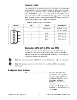
Страница 14: ...re for voltage sensing only Providing current through these pins may damage the backplane If your power supply has voltage sensing use these pins otherwise leave them unconnected Pins with power plane in the description are connected to the backplane s internal power planes and are suitable for carrying current Note Tyco Electronics manufactures the J205 mating connector which you can order with p...

Страница 15: ...2 V sense only no power No 11 GND Ground plane Yes 12 12V 12 V power plane Yes 13 GND Ground plane No 14 OVERTEMP Alert of over temperature condition in card cage No 15 GND Ground plane No 16 LED1 J200 pin 3 No 17 LED2 J200 pin 4 No 18 5V_SENSE 5 V sense only no power No 19 GND Ground plane No 20 GND Ground plane No 21 GND Ground plane No 22 SMBCLK Backplane SMBus clock No 23 SMBDAT Backplane SMBu...

Страница 16: ...th part number CBD7W2M2000Z 759 1 Figure 10 J206 Connector 29 GND Ground plane Yes 30 PS_ON From system slot J20 pin D2 No 31 12V_FAN To test point E8 No 32 GND Ground plane Yes 33 PS_OK To system slot from power supply Yes 34 GND Ground plane Yes 35 GND Ground plane Yes 36 3 3V 3 3 V power plane Yes 37 5V 5 V power plane Yes Table 2 Connector J205 Pin Descriptions Continued Connector Pin Signal D...

Страница 17: ...nectors for four thermistors to monitor the card cage temperature You can use signal OVERTEMP on J205 as an alarm indicating when the card cage temperature exceeds 90 C when used in conjunction with the four thermistors Note Use a Sensor Scientific KWM502C 6 or similar thermistor with these connectors Note The mating connector for J213 J214 J215 and J216 is Molex part number 50 57 9402 Backplane S...

Страница 18: ...z 1 MHz range Duty factor 45 55 Unloaded signal swing 3 3 V 0 3 V Note For other specifications refer to the PXI 1 Hardware Specification 100 MHz System Reference Clock PXIe_CLK100 and PXIe_SYNC100 Maximum slot to slot skew 100 ps Accuracy 25 ppm max guaranteed over the operating temperature range Maximum jitter 3 ps RMS phase jitter 10 Hz 12 kHz range 2 ps RMS phase jitter 12 kHz 20 MHz range Dut...

Страница 19: ...100 PPM Input amplitude J206 200 mVPP to 5 VPP square wave or sine wave System timing slot PXI_CLK10_IN 5 V or 3 3 V TTL signal J206 input impedance 50 Ω 5 Ω Maximum jitter introduced by backplane 1 ps RMS phase jitter 10 Hz 1 MHz range PXIe_SYNC_CTRL VIH 2 0 5 5 V VIL 0 0 8 V PXI Star Trigger Maximum slot to slot skew 250 ps Backplane characteristic impedance 65 Ω 10 Notes For PXI slot to PXI Sta...

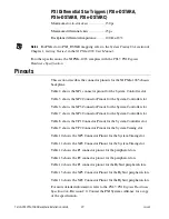
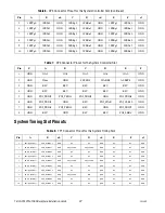
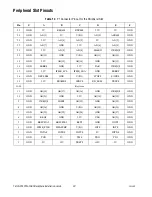
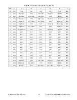
Страница 20: ...ble 6 shows the XP3 Connector Pinout for the System Controller slot Table 7 shows the XP4 Connector Pinout for the System Controller slot Table 8 shows the TP1 Connector Pinout for the System Controller slot Table 9 shows the TP2 Connector Pinout for the System Timing slot Table 10 shows the XP3 Connector Pinout for the System Timing slot Table 11 shows the XP4 Connector Pinout for the System Timi...

Страница 21: ...Tp0 4PETn0 GND 4PERp0 4PERn0 GND 4PETp1 4PETn1 GND 4 4PETp2 4PETn2 GND 4PERp2 4PERn2 GND 4PERp1 4PERn1 GND 5 4PETp3 4PETn3 GND 4PERp3 4PERn3 GND RSV RSV GND 6 RSV RSV GND RSV RSV GND RSV RSV GND 7 RSV RSV GND RSV RSV GND RSV RSV GND 8 RSV RSV GND RSV RSV GND RSV RSV GND 9 RSV RSV GND RSV RSV GND RSV RSV GND 10 RSV RSV GND RSV RSV GND RSV RSV GND Table 6 XP3 Connector Pinout for the System Controll...

Страница 22: ...RIG6 GND 6 GND PXI_TRIG2 GND RSV PXI_STAR PXI_CLK10 GND 7 GND PXI_TRIG1 PXI_TRIG0 RSV GND PXI_TRIG7 GND 8 GND RSV GND RSV RSV PXI_LBR6 GND Table 8 TP1 Connector Pinout for the System Timing Slot Pin A B ab C D cd E F ef 1 PXIe_DSTARA3 PXIe_DSTARA3 GND NC NC GND NC NC GND 2 PXIe_DSTARC4 PXIe_DSTARC4 GND PXI_STAR12 PXI_STAR13 GND NC NC GND 3 PXIe_DSTARB4 PXIe_DSTARB4 GND NC NC GND NC NC GND 4 PXIe_D...

Страница 23: ...0 XP3 Connector Pinout for the System Timing Slot Pin A B ab C D cd E F ef 1 PXIe_CLK100 PXIe_CLK100 GND PXIe_SYNC100 PXIe_SYNC100 GND PXIe_DSTARC PXIe_DSTARC GND 2 PRSNT PWREN GND PXIe_DSTARB PXIe_DSTARB GND PXIe_DSTARA PXIe_DSTARA GND 3 SMBDAT SMBCLK GND RSV RSV GND RSV RSV GND 4 MPWRGD PERST GND RSV RSV GND 1RefClk 1RefClk GND 5 1PETp0 1PETn0 GND 1PERp0 1PERn0 GND 1PETp1 1PETn1 GND 6 1PETp2 1PE...

Страница 24: ...AD 14 GND AD 13 GND 18 GND SERR GND 3 3V PAR C BE 1 GND 17 GND 3 3V IPMB_SCL IPMB_SDA GND PERR GND 16 GND DEVSEL GND V I O STOP LOCK GND 15 GND 3 3V FRAME IRDY BD_SEL TRDY GND 12 14 Key Area 11 GND AD 18 AD 17 AD 16 GND C BE 2 GND 10 GND AD 21 GND 3 3V AD 20 AD 19 GND 9 GND C BE 3 IDSEL AD 23 GND AD 22 GND 8 GND AD 26 GND V I O AD 25 AD 24 GND 7 GND AD 30 AD 29 AD 28 GND AD 27 GND 6 GND REQ GND 3 ...

Страница 25: ...PXI_STAR PXI_CLK10 GND 16 GND PXI_TRIG1 PXI_TRIG0 RSV GND PXI_TRIG7 GND 15 GND PXI_BRSVA15 GND RSV PXI_LBL6 PXI_LBR6 GND 14 GND RSV RSV RSV GND RSV GND 13 GND RSV GND V I O RSV RSV GND 12 GND RSV RSV RSV GND RSV GND 11 GND RSV GND V I O RSV RSV GND 10 GND RSV RSV RSV GND RSV GND 9 GND RSV GND V I O RSV RSV GND 8 GND RSV RSV RSV GND RSV GND 7 GND RSV GND V I O RSV RSV GND 6 GND RSV RSV RSV GND RSV ...

Страница 26: ...4 GND AD 13 GND 18 GND SERR GND 3 3V PAR C BE 1 GND 17 GND 3 3V IPMB_SCL IPMB_SDA GND PERR GND 16 GND DEVSEL GND V I O STOP LOCK GND 15 GND 3 3V FRAME IRDY BD_SEL TRDY GND 12 14 Key Area 11 GND AD 18 AD 17 AD 16 GND C BE 2 GND 10 GND AD 21 GND 3 3V AD 20 AD 19 GND 9 GND C BE 3 IDSEL AD 23 GND AD 22 GND 8 GND AD 26 GND V I O AD 25 AD 24 GND 7 GND AD 30 AD 29 AD 28 GND AD 27 GND 6 GND REQ GND 3 3V C...

Страница 27: ...Tn1 GND 6 1PETp2 1PETn2 GND 1PERp2 1PERn2 GND 1PERp1 1PERn1 GND 7 1PETp3 1PETn3 GND 1PERp3 1PERn3 GND 1PETp4 1PETn4 GND 8 1PETp5 1PETn5 GND 1PERp5 1PERn5 GND 1PERp4 1PERn4 GND 9 1PETp6 1PETn6 GND 1PERp6 1PERn6 GND 1PETp7 1PETn7 GND 10 RSV RSV GND RSV RSV GND 1PERp7 1PERn7 GND Table 16 XP4 Connector Pinout for the Hybrid Slot Pin Z A B C D E F 1 GND GA4 GA3 GA2 GA1 GA0 GND 2 GND 5Vaux GND SYSEN WAK...

Страница 28: ...Other product and company names mentioned herein are trademarks or trade names of their respective companies For patents covering National Instruments products technology refer to the appropriate location Help Patents in your software the patents txt file on your media or the National Instruments Patent Notice at ni com patents 2008 National Instruments Corporation All rights reserved 372640A 01 S...

Отзывы: