Index
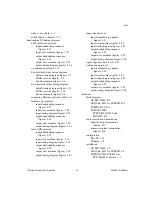
I-8
ni.com
installation, 1-7
support for DMA transfers (table), E-3
PCLK<1..2> signal
burst input timing diagrams
PCLK reversed (figure), 3-9
transfer example (figure), 3-6
burst output timing diagrams
output timing diagram (figure), 3-8
PCLK reversed (figure), 3-10
transfer example (figure), 3-6
description (table), C-4
frequency selection for programmable
handshaking I/O and pattern I/O
signal direction for burst protocol, 2-18
phase-locked loop circuit
block diagram, D-11
description, D-10
physical specifications, A-4
pin assignments
50-pin signal connections (figure), C-6
68-pin signal connections (figure), C-2
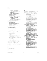
PLL.
See
phase-locked loop circuit, D-10
polarity
comparison of handshaking protocols
controlling line polarities, 2-23
Port 4 lines (table), 2-4
ports, configuring, 2-6
power connections, D-5
power specifications
power available at I/O connector, A-4
power requirements, A-4
power-on state, D-5
programmable delay, handshaking
programming
software programming choices
change detection
continuous change detection in
single buffer change detection in
handshaking I/O
buffered handshaking I/O in NI-DAQ
LabVIEW/LabVIEW RT
(figure), 2-26
LabVIEW/LabVIEW RT
(figure), 2-27
pattern I/O
continuous, in NI-DAQ (figure), 2-15
LabVIEW/LabVIEW RT
unstrobed I/O
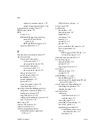
programming examples (NI resources), F-1
PXI bus interface.
See
RTSI and PXI trigger
bus interfaces
PXI, using with CompactPCI, B-1
PXI-6533 device
benchmark results (table), E-6
installation, 1-7
support for DMA transfers (table), E-3
with LabVIEW RT, E-10
PXI-6534 device
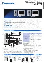
Содержание NI 653 Series
Страница 1: ...PCI 6533...


