background image

Chapter 3

Timing Diagrams

NI 653X User Manual

3-22

ni.com

Using Protocols Based on Signal Edges

The NI 653

X

 can communicate using pulses on the ACK and REQ lines. 

The three edge protocols are:

Trailing-edge protocol—The trailing edge of the ACK or REQ pulse 
indicates that the NI 653

X

 or peripheral device is ready for a transfer.

Leading-edge protocol—The rising edge of the ACK or REQ pulse 
indicates that the NI 653

X

 or peripheral device is ready for a transfer.

Long-pulse protocol—This protocol is a variant of the leading-edge 
protocol, with the additional option of using a data-settling delay. If 
your application requires a large minimum pulse width, use this 
protocol. In this case, the programmable delay is used to increase the 
ACK pulse width instead of delaying the ACK pulse.

You can also use long-pulse protocol to handshake with an actual 8255 or 
82C55 PPI. You must set the ACK and REQ signals to active low and select 
a minimum pulse width of 500 ns for your 8255 or 82C55.

Using the Trailing-Edge Protocol

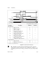
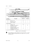
Figure 3-20.  

Trailing-Edge Input Handshaking Sequence

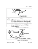
Reference 

Point

Action Steps

Initial State

ACK is deasserted. The NI 653

X

 waits for the peripheral device to pulse REQ to 

indicate it has data.

1

The NI 653

X

 sends an ACK pulse of programmable width when ready to receive 

data.

2

After receiving the trailing edge of the ACK pulse, the peripheral device can 
strobe data into the NI 653

X

 and pulse the REQ.

3

The NI 653

X

 sends another ACK pulse when ready for another input.

ACK

REQ

2

1

ACK and REQ are shown as active high.

Steps 1–2 are repeated for each transfer.

3

Initial State

Data Latched

Data Valid

Содержание NI 653 Series

Страница 1: ...PCI 6533...

Страница 2: ...DAQ NI 653X User Manual for Traditional NI DAQ High Speed Digital I O Devices for PCI PXI CompactPCI AT EISA and PCMCIA Bus Systems NI 653X User Manual February 2005 371464D 01...

Страница 3: ...rea 82 02 3451 3400 Lebanon 961 0 1 33 28 28 Malaysia 1800 887710 Mexico 01 800 010 0793 Netherlands 31 0 348 433 466 New Zealand 0800 553 322 Norway 47 0 66 90 76 60 Poland 48 22 3390150 Portugal 351...

Страница 4: ...gligent acts and power failure or surges fire flood accident actions of third parties or other events outside reasonable control Copyright Under the copyright laws this publication may not be reproduc...

Страница 5: ...t of Communications DOC Changes or modifications not expressly approved by NI could void the user s authority to operate the equipment under the FCC Rules Class A Federal Communications Commission Thi...

Страница 6: ...rash When this symbol is marked on a product refer to the for information about precautions to take bold Bold text denotes items that you must select or click in the software such as menu items and di...

Страница 7: ...DAQCard 6533 for PCMCIA 1 9 Configuring the NI 653X 1 9 In Windows 1 9 In Mac OS 1 10 Safety Information 1 10 Chapter 2 Using Your NI 653X Choosing the Correct Mode for Your Application 2 1 Controllin...

Страница 8: ...2 18 Selecting ACK REQ Signal Polarity 2 19 Choosing Whether to Use a Programmable Delay 2 19 Choosing Continuous or Finite Data Transfer 2 20 Finite Transfers 2 20 Continuous Input 2 20 Continuous O...

Страница 9: ...sing the Burst Protocol 3 5 Using Asynchronous Protocols 3 11 Using the 8255 Emulation Protocol 3 11 Using the Level ACK Protocol 3 17 Using Protocols Based on Signal Edges 3 22 Using the Trailing Edg...

Страница 10: ...of current The NI 6534 contains onboard memory enabling you to transfer data to from this memory at a guaranteed rate This memory removes the dependency on the host computer bus for applications that...

Страница 11: ...tions Control Lines In addition to controlling and monitoring relay type applications the NI 653X also provides two timing handshaking controllers named Group 1 and Group 2 for high speed data transfe...

Страница 12: ...is included with LabVIEW The LabVIEW Data Acquisition VI Library is functionally equivalent to the NI DAQ application programming interface API As with LabVIEW you develop your LabVIEW RT applications...

Страница 13: ...are The NI DAQ driver software shipped with your NI 653X has an extensive library of functions that you can call from your ADE These functions allow you to use all the features of the NI 653X NI DAQ c...

Страница 14: ...s are compatible with your device Table 1 1 NI 653X Devices and NI DAQ Support Device Supported NI DAQ Version Windows Mac NI PCI DIO 32HS Version 5 0 or later Version 6 1 0 or later NI AT DIO 32HS Ve...

Страница 15: ...To avoid such damage in handling the device take the following precautions Ground yourself using a grounding strap or by holding a grounded object Touch the antistatic package to a metal part of your...

Страница 16: ...r computer chassis to discharge any static electricity that might be on your clothes or body 5 Insert the NI 653X into a PCI system slot It may be a tight fit but do not force the device into place 6...

Страница 17: ...fully inject the device into place 6 Screw the front panel of the NI PXI 653X to the front panel mounting rails of the PXI or CompactPCI chassis 7 Visually verify the installation Make sure the device...

Страница 18: ...ve the PCMCIA slot cover on your computer if any You are now ready to configure your NI 653X Configuring the NI 653X Your NI 653X is automatically configured in Measurement Automation Explorer MAX whi...

Страница 19: ...an work in the system Now that you have completed configuring your device you can begin setting up the device for use Safety Information The following section contains important safety information tha...

Страница 20: ...tor blocks when power is connected to the system Avoid contact between your body and the connector block signal when hot swapping modules Remove power from signal lines before connecting them to or di...

Страница 21: ...ts performed on household appliances portable tools and similar product Installation Category III is for measurements performed in the building installation at the distribution level This category ref...

Страница 22: ...rform basic digital I O that does not need hardware timing or handshaking between the NI 653X and the peripheral device Unstrobed I O I want to individually configure the direction of each bit instead...

Страница 23: ...resistors It is independent of the state of the DPULL line which selects whether the 653X pulls the data lines high or low when undriven It has high current drive for both its logic high and logic low...

Страница 24: ...s Generate or receive digital patterns and waveforms at regular intervals or timed by an external TTL signal Transfer data between two devices using one of six configurable handshaking protocols Acqui...

Страница 25: ...ing a Program Using the following flowcharts as a guide create a program to perform unstrobed I O Figure 2 1 displays a flowchart for C programming using NI DAQ and Figure 2 2 shows a LabVIEW programm...

Страница 26: ...erface If both sets of control timing lines are available call DIG_In_Prt or DIG_Out_Prt and set Port Number to 4 If both sets of control timing lines are not available use DIG_In_Line and DIG_Out_Lin...

Страница 27: ...ceiving Digital Patterns and Waveforms Pattern I O Using pattern I O you can acquire or generate patterns on every rising or falling edge of a clock signal The clock signal can be generated internally...

Страница 28: ...xternal REQ source is transferred on the rising edge of the signal and on the falling edge of the internal REQ source You can reverse the REQ polarity by using the following functions NI DAQ C interfa...

Страница 29: ...he software chooses the closest transfer rate by selecting the frequency and divisor To see the actual transfer rate create an indicator at the actual clock frequency output of Digital Clock Config VI...

Страница 30: ...data is acquired NI DAQ returns an error Figure 2 4 Stopping Data Transfer Using a Trigger Start and Stop Trigger When you use a start and stop trigger data transfer starts upon receiving a trigger o...

Страница 31: ...attern comparison 0 for bits not of interest The polarity whether to trigger on data that matches or mismatches the specified pattern For example if you want to start acquisition when the two least si...

Страница 32: ...an allow the device to continue acquiring when it runs out of buffer space and overwrite data you have not yet read You can specify this through the oldDataStop parameter in the DIG_DB_Config function...

Страница 33: ...t data the buffer size must be an even number There are no restrictions for 32 bit data For 8 or 16 bit data you may need to add dummy data to the buffer to make it the correct size Choosing DMA or In...

Страница 34: ...or 68 Pin Assignments or Figure C 2 68 to 50 Pin Adapter Pin Assignments If you are using an external source for your REQ signal connect it to the appropriate REQ pin of the I O connector If you are u...

Страница 35: ...mming using NI DAQ while Figure 2 9 shows a LabVIEW programming flowchart The boxes represent function names for the appropriate software and the diamonds represent decision points Figure 2 7 Programm...

Страница 36: ...e 2 8 Programming Pattern I O Continuous in NI DAQ C API DIG_DB_HalfReady Is the next half buffer ready DIG_DB_Transfer DIG_Block_Clear Acquisition Complete Yes Yes No No Yes No DIG_Block_In DIG_Block...

Страница 37: ...preloads the onboard memory with data before starting the output operation Preloading eliminates or reduces the impact of the PCI bus bandwidth limitations and increases the overall transfer rate The...

Страница 38: ...ing I O mode Choosing the Width of Data to Transfer You can choose between a width of 8 16 or 32 bits Use the following table to find the valid combinations of ports and timing controllers you can use...

Страница 39: ...3 Timing Diagrams for more information about the burst protocol If you want to acquire or generate patterns of every edge of a clock signal refer to the Generating and Receiving Digital Patterns and...

Страница 40: ...cur faster than the peripheral device can handle For all protocols except burst the delay increases the time before the NI 653X can respond to the REQ signal For the burst protocol the programmable de...

Страница 41: ...n and the data overwrite regen parameter in the Digital Buffer Control VI called by the DIO Start VI Continuous Output Similarly with continuous output the NI 653X continuously reads data from compute...

Страница 42: ...data to the buffer to make it the correct size Choosing DMA or Interrupt Transfers When using DMA default the NI 6534 transfers data in 32 byte blocks and the NI 6533 transfers data in 4 byte blocks...

Страница 43: ...g a valid ACK value before you enable the transfer on the peripheral device Similarly you can make sure the peripheral device is configured and is driving a valid REQ value before you enable the trans...

Страница 44: ...undriven control line state of the REQ and ACK lines is low If you want to change state to high use one of the three following methods Use the CPULL bias selection line and connect the CPULL pin on th...

Страница 45: ...n NI DAQ C API Read DIG_Grp_Mode DIG_Grp_Config Read Continuous No DIG_DB_Config Yes DIG_Block_In DIG_Block_Out DIG_Block_In DIG_Block_Out Yes No Yes No Yes DIG_DB_HalfReady Is the next half buffer re...

Страница 46: ...Manual Figure 2 12 Programming Unbuffered Handshaking I O in NI DAQ C API DIG_Grp_Config Input DIG_Grp_Mode DIG_Grp_Status Ready DIG_In_Grp DIO_Grp_Config Done DIG_Out_Grp DIG_Grp_Status Ready Done D...

Страница 47: ...DIO Start VI DIO Parameter VI DIO Clear VI Buffered Operation DIO Config VI Yes Burst Mode No No No Reverse PCLK Direction Yes Yes Finite Buffer DIO Read VI Yes Done DIO Read VI Yes No No Digital Sing...

Страница 48: ...n Preloading the memory eliminates or reduces the impact of the PCI bus bandwidth limitations and increases the overall transfer rate DIO Start VI DIO Parameter VI DIO Clear VI Buffered Operation DIO...

Страница 49: ...xternal device Monitoring Line State Change Detection You can configure your NI 653X to acquire data whenever the state of one or more data lines change Once the NI 653X detects a change in one of the...

Страница 50: ...f a port Pattern 1 does not have changes in the two bits of interest and data is not latched For pattern 2 however a change is detected on one of the two bits of interest and the value of the entire p...

Страница 51: ...d stop trigger Start Trigger A start trigger is a trigger that initiates a pattern I O upon receipt of a hardware trigger on the ACK STARTTRIG pin Figure 2 16 Starting Data Transfer Using a Trigger St...

Страница 52: ...operation once a user specified digital pattern is matched Specify four parameters to set a pattern matching trigger Whether it is a start or stop trigger The data pattern to be detected matched The m...

Страница 53: ...a to a computer memory buffer and stops the operation Continuous Input For continuous input the NI 653X continuously transfers input data to the computer memory buffer As the device fills the buffer c...

Страница 54: ...ime from the computer than DMA driven transfers Connecting Signals Connect digital input signals to the I O connector using the pinout diagrams Figure C 1 NI 653X I O Connector 68 Pin Assignments or F...

Страница 55: ...in NI DAQ C API DIG_DB_HalfReady Is the next half buffer ready DIG_DB_Transfer DIG_Block_Clear Acquisition Complete Yes Yes No No DIG_Grp_Config DIG_Trigger_Config DIG_DB_Config DIG_Block_PG_Config DI...

Страница 56: ...onal Instruments Corporation 2 35 NI 653X User Manual Figure 2 22 Programming Change Detection for NI DAQ LabVIEW LabVIEW RT API DIO Config VI Done DIO Clear VI Yes No DIO Start VI Specify Data Mask H...

Страница 57: ...ich can lower your transfer rate For more information about transfer rates refer to Appendix E Optimizing Your Transfer Rates Internal REQ Signal Source The NI 653X can internally generate a signal RE...

Страница 58: ...data on the I O pins on the falling edge of the REQ signal The low time and high time of the REQ signal must each be 20 ns The minimum duration for a period of the REQ signal is 50 ns Parameter Descr...

Страница 59: ...ords assert STARTTRIG at least 15 ns before the start of the REQ pulse The STARTTRIG signal is synchronized to the REQ edge using a flip flop Because of this synchronization flip flop there is a one R...

Страница 60: ...Table 3 1 Note Whether an ACK or a REQ signal occurs first in the handshaking sequence depends on the protocol and the transfer direction Table 3 1 Handshaking Protocol Characteristics Protocol REQ A...

Страница 61: ...CLK line The NI 653X asserts the ACK signal if it is ready to perform a transfer If the peripheral device also asserts the REQ signal indicating it is ready a transfer occurs on the rising edge of the...

Страница 62: ...both the NI 653X and the peripheral device are ready and thus ACK and REQ are asserted so it is not reasonable to expect data to arrive at consistent intervals If consistent intervals are an important...

Страница 63: ...Diagram Default Parameter Description Minimum Maximum Input Parameters trs Setup time from REQ valid to PCLK 12 trh Hold time from PCLK to REQ invalid 0 tdis Setup time from input data valid to PCLK 4...

Страница 64: ...ation 20 tpl PCLK low pulse duration 20 trs Setup time from REQ valid to PCLK falling edge 1 trh Hold time from PCLK to REQ invalid 0 Output Parameters tpa PCLK to ACK valid 22 tah Hold time from PCLK...

Страница 65: ...duration 20 tpl PCLK low pulse duration 20 trs Setup time from REQ valid to PCLK falling edge 1 trh Hold time from PCLK to REQ invalid 0 tdis Setup time from input data valid to PCLK falling edge 0 t...

Страница 66: ...uration tpc 2 5 tpc 2 5 tpa PCLK to ACK valid 18 tah Hold time from PCLK to ACK invalid 3 tpdo PCLK to output data valid 28 tdoh Hold time from PCLK to output data invalid 4 tdis Setup time from input...

Страница 67: ...ector on the active REQ edge before reading the data For output after writing the data the NI 653X latches data out of the I O connector on the active REQ edge The active edge of the REQ is determined...

Страница 68: ...andshaking Sequence Reference Point Action Steps 1 The NI 653X asserts the ACK signal when ready to accept data 2 The peripheral device can then strobe data into the NI 653X by asserting the REQ line...

Страница 69: ...X User Manual Figure 3 10 8255 Emulation Input State Machine Wait for Space Wait For REQ Programmable Delay Wait for REQ When REQ is unasserted latch input data When NI 6533 Device has space for data...

Страница 70: ...t 5 The rising REQ signal edge enables a new transfer to occur The peripheral device should wait until it has received data before deasserting the REQ signal The peripheral device can also wait for th...

Страница 71: ...3X User Manual Figure 3 12 8255 Emulation Output State Machine Wait For Data Wait For REQ Programmable Delay Wait For REQ When REQ Unasserted When 6533 Device has data to output output data When REQ A...

Страница 72: ...REQ rising edge 0 tdir Input data valid to REQ rising edge 0 trdi REQ rising edge to input data invalid 10 Output Parameters taa ACK high duration 100 tr a REQ falling edge to ACK rising edge 150 tdoa...

Страница 73: ...il the peripheral asserts REQ the peripheral may either pulse REQ or hold REQ high until the first ACK occurs If the peripheral pulses REQ make sure to start the transfer on the NI 653X before the pul...

Страница 74: ...ne Wait For Space Wait For REQ Programmable Delay Programmable Delay Wait For REQ When REQ Asserted Clear ACK When 6533 Device has space for data input data When REQ Unasserted Initial State ACK Clear...

Страница 75: ...inimum Maximum Input Parameters trr REQ pulse width 75 tr r REQ inactive duration 75 tar ACK to next REQ 0 tdir 1 Input data setup to REQ active with REQ edge latching 0 trdi Input data hold from REQ...

Страница 76: ...ctive going REQ occurs Since the REQ is already asserted the NI 653X waits until REQ deasserts and reasserts to deassert the ACK signal and request additional data 3 The asserted REQ signal deasserts...

Страница 77: ...ximum Input Parameters trr REQ pulse width 75 tr r REQ inactive duration 75 tar ACK to next REQ 0 Output Parameters taa ACK pulse width 225 tra REQ to ACK inactive 100 200 tr do REQ inactive to new ou...

Страница 78: ...is used to increase the ACK pulse width instead of delaying the ACK pulse You can also use long pulse protocol to handshake with an actual 8255 or 82C55 PPI You must set the ACK and REQ signals to act...

Страница 79: ...ut State Machine Wait For Space Wait For REQ Programmable Delay Programmable Delay Wait For REQ When REQ Unasserted When 6533 Device has space for data input data Clear ACK When REQ Asserted Send ACK...

Страница 80: ...nput Parameters trr REQ pulse width 75 tr r REQ inactive duration 75 tdir Input data setup to REQ inactive with REQ edge latching 0 tr di Input data hold from REQ inactive with REQ edge latching 10 td...

Страница 81: ...lse deasserts the ACK signal if it has not previously been deasserted and requests additional data ACK REQ 2 1 ACK and REQ are shown as active high Steps 1 2 are repeated for each transfer Initial Sta...

Страница 82: ...eters trr REQ pulse width 75 tr r REQ inactive duration 75 ta r ACK inactive to next REQ inactive 0 Output Parameters taa ACK pulse width 2251 2752 tr do 1 REQ inactive to new output data with REQ edg...

Страница 83: ...es REQ make sure to start the transfer on the NI 653X before the pulse occurs to avoid missing the pulse 1 The NI 653X sends an ACK pulse when it is ready to receive data The ACK pulse width is fixed...

Страница 84: ...ait For Space Wait For REQ Programmable Delay Programmable Delay Wait For REQ When REQ Asserted When 6533 Device has space for data input data Clear ACK Pulse When REQ Unasserted Initial State ACK Cle...

Страница 85: ...um Input Parameters trr REQ pulse width 75 tr r REQ inactive duration 75 tar ACK to next REQ 0 tdir 1 Input data setup to REQ active with REQ edge latching 0 trdi Input data hold from REQ active with...

Страница 86: ...ce deasserts the REQ signal 2 Once the data is latched the peripheral device must respond with an active going REQ signal edge to request additional data 3 To slow down the data transfer you can inser...

Страница 87: ...imum Input Parameters trr REQ pulse width 75 tr r REQ inactive duration 75 tar ACK to next REQ 0 Output Parameters taa ACK pulse width 150 tr a REQ inactive to ACK inactive 150 tr do REQ inactive to n...

Страница 88: ...avoid missing the pulse 1 The NI 653X asserts an ACK signal when it is ready to receive data assuming the peripheral device has deasserted the REQ signal Otherwise the ACK signal remains asserted unti...

Страница 89: ...te Machine Wait For Space Wait For REQ Programmable Delay Programmable Delay Wait For REQ When REQ Asserted When 6533 Device has space for data input data Clear ACK Pulse When REQ Unasserted Initial S...

Страница 90: ...s trr REQ pulse width 75 tr r REQ inactive duration 75 tar ACK to next REQ 0 tdir 1 Input data setup to REQ active with REQ edge latching 0 trdi Input data hold from REQ active with REQ edge latching...

Страница 91: ...peripheral device can latch the data on the rising or falling edge of the ACK pulse or it can latch the data any time before asserting the REQ signal 3 When the data is latched the peripheral device...

Страница 92: ...Maximum Input Parameters trr REQ pulse width 75 tr r REQ inactive duration 75 tar ACK to next REQ 0 Output Parameters taa ACK pulse width 1251 tr do REQ inactive to new output data with REQ edge latc...

Страница 93: ...32 input output 4 dedicated output and control 4 dedicated input and status Compatibility TTL CMOS standard or open collector Hysteresis 500 mV Digital logic levels Level Min Max Input low voltage 0...

Страница 94: ...533 for PCMCIA 16 S NI PCI PXI 6534 64 MB two 32 MB modules on each NI 6534 NI PCI PXI 7030 6533 16 S NI PCI DIO 32HS 16 S NI PXI 6533 16 S Input high current for control lines Vin 2 4 V CPULL high CP...

Страница 95: ...mpatibility TTL CMOS Trigger types Rising or falling edge or digital pattern Pulse width for edge triggers min 10 ns Pattern trigger detection capabilities Detect pattern match or mismatch on user sel...

Страница 96: ...A NI DAQCard 6533 for PCMCIA 4 65 to 5 25 VDC at 250 mA Physical Dimensions not including connectors NI DAQCard 6533 for PCMCIA 8 6 by 5 3 cm 3 4 by 2 1 in NI AT DIO 32HS PCI 653X 17 5 by 10 7 cm 6 9...

Страница 97: ...peak 30 shocks per face Operational random vibration PXI only 5 to 500 Hz 0 31 grms 3 axes Nonoperational random vibration PXI only 5 to 500 Hz 2 5 grms 3 axes Note Random vibration profiles were deve...

Страница 98: ...does not include these sub buses Your NI PXI 653X works in any standard CompactPCI chassis adhering to the PICMG CompactPCI 2 0 R2 1 document PXI specific features are implemented on the J2 connector...

Страница 99: ...f your data transfer when using the handshaking and pattern I O modes The direction and function of each signal varies depending on the mode of operation as shown in Table C 1 Table C 1 Control Signal...

Страница 100: ...ections Figure C 1 NI 653X I O Connector 68 Pin Assignments 5 V REQ1 ACK1 STARTTRIG1 STOPTRIG1 PCLK1 PCLK2 STOPTRIG2 ACK2 STARTTRIG2 REQ2 DIOA0 GND DIOA3 DIOA4 GND DIOA7 DIOB0 DIOB1 GND RGND GND DIOB6...

Страница 101: ...form handshaking I O between two NI 653X devices using an SH 68 68 D1 cable Use Table C 2 to find the accessories designed for connecting signals to your NI 653X Signal Descriptions Use Table C 3 to f...

Страница 102: ...O Option to use the ACK 1 2 lines as extra general purpose output lines OUT 3 4 4 7 STOPTRIG 1 2 Control Group 1 and group 2 stop triggers Handshaking I O Not used Pattern I O Used in trigger operati...

Страница 103: ...ull down selection Input signal that selects whether the NI 653X pulls the data lines DIOA DIOB DIOC and DIOD up or down when the lines are not driven If you connect DPULL to 5 V on the external termi...

Страница 104: ...DIOB0 DIOB7 DIOB5 DIOA7 DIOA1 DIOA0 DIOA4 REQ1 PCLK1 OUT1 STOPTRIG1 IN1 ACK1 GND GND GND GND GND DIOC6 DIOC2 DIOC3 DIOC5 DIOD2 DIOD6 DIOD3 DIOD1 DIOB1 DIOB6 DIOB2 DIOA3 DIOA2 DIOA6 GND DIOB3 DIOA5 GN...

Страница 105: ...es and cable assemblies shielded and ribbon Connector blocks shielded and unshielded 50 and 68 pin screw terminals RTSI bus cables for AT and PCI devices SCXI modules and accessories that can acquire...

Страница 106: ...erstand how your NI 653X hardware works Block Diagrams Figure D 1 NI AT DIO 32HS Block Diagram DAQ DIO Counters and Timers DMA Interrupt Requests Handshaking and Control Data Latches and Drivers Data...

Страница 107: ...PCMCIA Block Diagram DAQ DIO Counters and Timers DMA Interrupt Requests Handshaking and Control Data Latches and Drivers Data Lines Data Lines 32 16 PCMCIA Interface PCMCIA I O Channel Control Lines 8...

Страница 108: ...NIPXI 6533BlockDiagram DAQ DIO Counters and Timers DMA Interrupt Requests Handshaking and Control Data Latches and Drivers Data Lines Data Lines 32 32 MITE PCI Interface PCI I O Channel EEPROM RTSI PX...

Страница 109: ...FIFOs Bus Interface DMA IRQ Counter and Timers Clock Selection DAQ DIO Bus Interface SCARAB Interface SCARAB Interface FPGA MITE Interface DMA IRQ Handshaking and Control RTSI Interface Data Lines 32...

Страница 110: ...ull down Caution Do not connect CPULL DPULL or any other line directly to an external power supply while the NI 653X is powered off This action may prevent your computer from booting For example if yo...

Страница 111: ...transmission line For more information about this cable and other accessories refer to Appendix C Connecting Signals with Accessories Tip Cables that do not meet the above requirements such as ordina...

Страница 112: ...5 V connection through a long wire back to the 5 V pin of the NI 653X add a capacitor to your termination circuit to stabilize the 5 V connection near the Schottky diodes One suitable Schottky diode...

Страница 113: ...rate of the NI 653X or the characteristic impedance of the SH6868 D1 cable However the following information might be helpful I O buffers The NI 653X uses 24 mA rate controlled TTL level CMOS drivers...

Страница 114: ...ht angles to each other Do not run signal lines through conduits that also contain power lines How Much Current Can I Sink or Source Make sure the sink current does not exceed 24 mA at 0 4 V to guaran...

Страница 115: ...tPCI chassis Board RTSI and PXI Bus Clocks The NI 653X requires a clock to run the handshaking logic and to generate sampling intervals for pattern I O The frequency timebase must be 20 MHz The NI 653...

Страница 116: ...PLL circuit is automatically enabled when the NI PXI 6534 is powered on No configuration steps are required in order to utilize PLL synchronization Figure D 6 PLL Circuit Block Diagram RTSI and PXI B...

Страница 117: ...iderations NI 653X User Manual D 12 ni com Figure D 7 RTSI Bus Signal Connection RTSI Bus or PXI Connector Crossbar Switch Trigger 20 MHz Timebase REQ 1 2 ACK 1 2 STARTTRIG 1 2 PCLK 1 2 DAQ DIO STOPTR...

Страница 118: ...rate is always lower than the peak transfer rate The average bus bandwidth requirements differ between specific NI 653X devices Here the NI 653X devices are listed in order of their average bus bandwi...

Страница 119: ...mory If you are using an NI 6533 you can connect it to an external FIFO using the burst handshaking protocol and clock data out of the FIFO to the peripheral device Output looping from the NI 6534 onb...

Страница 120: ...o MB s use the following formula where sample size can be one two or four bytes For example 10 MS s where each sample is 16 bits two bytes The following applications were tested Finite pattern I O and...

Страница 121: ...the application software NI AT DIO 32HS The following benchmarks are results using a Dell Dimension XPS 600 MHz PIII and Windows 98 SE Table E 3 NI AT DIO 32HS Benchmark Results Mode Benchmark Rate M...

Страница 122: ...nchmark Rate MS s 8 Bit Samples 16 Bit Samples 32 Bit Samples Pattern Input Finite 32 MB 10 5 5 64 MB 10 5 5 Pattern Output Finite 32 MB 5 2 22 2 22 64 MB 4 2 22 2 22 Pattern Input Continuous 1 GB 2 5...

Страница 123: ...les 16 Bit Samples 32 Bit Samples Pattern Input Finite 32 MB 10 5 5 64 MB 10 5 5 Pattern Output Finite 32 MB 5 2 857 2 857 64 MB 5 2 5 2 5 Pattern Input Continuous 1 GB 2 5 1 43 1 43 Pattern Output Co...

Страница 124: ...PIII and Windows 98 Table E 6 NI DAQCard 6533 for PCMCIA Benchmark Results Mode Benchmark Rate MS s 8 Bit Samples 16 Bit Samples 32 Bit Samples Pattern I O Single Shot Input 0 12 11 10 Output 0 12 12...

Страница 125: ...Rate MS s 8 Bit Samples 16 Bit Samples 32 Bit Samples Pattern Input Finite 32 MB 20 20 20 64 MB 20 20 20 Pattern Output Finite 32 MB 20 20 20 Pattern Input Continuous 1 GB 20 10 5 Pattern Output Conti...

Страница 126: ...MS s 8 Bit Samples 16 Bit Samples 32 Bit Samples Pattern Input Finite 32 MB 20 20 20 64 MB 20 20 20 Pattern Output Finite 32 MB 20 20 20 Pattern Input Continuous 1 GB 20 20 10 Pattern Output Continuo...

Страница 127: ...unning on LabVIEW RT Table E 9 NI PCI 7030 6533 Benchmark Results Mode Benchmark Rate MS s 8 Bit Samples 16 Bit Samples 32 Bit Samples Pattern I O Single Shot Input 1 82 95 49 Output 1 82 91 47 Patter...

Страница 128: ...11 NI 653X User Manual Pattern I O Continuous Retransmit Output 2 50 1 25 1 25 Burst Protocol Continuous Input 19 98 19 97 19 97 Output 19 97 17 72 8 60 Table E 10 NI PCI 7030 6533 Benchmark Results C...

Страница 129: ...truments Application Engineers make sure every question receives an answer For information about other technical support options in your area visit ni com services or contact your local office at ni c...

Страница 130: ...calibration If you searched ni com and could not find the answers you need contact your local office or NI corporate headquarters Phone numbers for our worldwide offices are listed at the front of thi...

Страница 131: ...ol Prefix Value k kilo 103 micro 10 6 m milli 10 3 M mega 106 n nano 10 9 Numbers Symbols degrees negative of or minus less than greater than less than or equal to greater than or equal to ohms per pe...

Страница 132: ...the property of a function that begins an operation and returns prior to the completion or termination of the operation B b bits B bytes bidirectional data lines Data lines that can be programmatical...

Страница 133: ...RIG REQ STOPTRIG and PCLK counter timer A circuit that counts external pulses or clock pulses timing CPULL A user configurable 2 2 k internal resistor for control lines You can connect the line to 5 V...

Страница 134: ...ent to the acceptor FIFOs are often used on DAQ devices to temporarily store incoming or outgoing data until that data can be retrieved or output For example an analog input FIFO stores the results of...

Страница 135: ...es interrupt A computer signal indicating that the CPU should suspend its current task to service a designated activity IOL current output high minimum amount of available current on the output pin wh...

Страница 136: ...aximum transfer rate of 132 MB s PCLK See control signals PCMCIA An expansion bus architecture that has found widespread acceptance as a de facto standard in notebook sized computers It originated as...

Страница 137: ...haking signal generated by the peripheral device indicating it is ready In some transfer modes the NI 653X can internally generate a REQ signal The REQ signal with a bar above the name indicates it is...

Страница 138: ...nt that is synchronized to a reference clock For software it is a property of a function that begins an operation and returns only when the operation is complete T tc cycle time th hold time tp propag...

Страница 139: ...used with a PC that has the functionality of a classic stand alone instrument 2 a LabVIEW software module VI which consists of a front panel user interface and a block diagram program Vin input voltag...

Страница 140: ...ence figure 3 14 output state machine figure 3 15 output timing diagram figure 3 16 overview 3 11 burst input timing diagrams default input timing diagram figure 3 7 PCLK reversed figure 3 9 transfer...

Страница 141: ...nsfers table E 3 B benchmark results See optimizing transfer rates block diagrams AT DIO 32HS D 1 DAQCard 6533 for PCMCIA D 2 PCI PXI 6534 D 4 PCI DIO 32HS PCI PXI 7030 6533 and PXI 6533 D 3 phase loc...

Страница 142: ...fers 2 21 finite 2 20 pattern I O continuous input 2 11 continuous output 2 11 DMA or interrupt transfers 2 12 finite 2 11 control lines Group 1 and Group 2 controllers 1 2 handshaking I O and pattern...

Страница 143: ...sources F 1 extra data lines using Group 1 and Group 2 control lines 2 3 F finite data transfer See continuous or finite data transfer G GND signal description table C 5 Group 1 and Group 2 introducti...

Страница 144: ...protocol input handshaking sequence figure 3 17 input state machine figure 3 18 input timing diagram figure 3 19 output handshaking sequence figure 3 20 output state machine figure 3 20 output timing...

Страница 145: ...se F 1 L LabVIEW and LabVIEW RT software 1 3 leading edge handshaking protocol comparison of protocols table 3 4 definition 3 22 input handshaking sequence figure 3 27 input state machine figure 3 28...

Страница 146: ...r finite data transfer continuous input 2 11 continuous output 2 11 DMA or interrupt transfers 2 12 finite 2 11 internal or external REQ source 2 7 maximum transfer rate table E 2 monitoring data tran...

Страница 147: ...ower connections D 5 power specifications power available at I O connector A 4 power requirements A 4 power on state D 5 programmable delay handshaking protocol 2 19 programming See also software prog...

Страница 148: ...e figure 3 27 input state machine figure 3 28 input timing diagram figure 3 29 output handshaking sequence figure 3 30 output state machine figure 3 30 output timing diagram figure 3 31 level ACK prot...

Страница 149: ...2 sink current D 9 software NI resources F 1 software installation 1 6 software programming choices National Instruments application software 1 3 NI DAQ driver software 1 4 source current D 9 specific...

Страница 150: ...n I O external REQ signal source 3 2 internal REQ signal source 3 1 trailing edge handshaking protocol comparison of protocols table 3 4 definition 3 22 input handshaking sequence figure 3 22 input st...

Страница 151: ...ing control timing lines as extra unstrobed data lines 2 5 flowcharts 2 5 using control lines as extra unstrobed data lines 2 3 when to use table 2 1 V voltage controlled crystal oscillator VCXO D 11...

Отзывы: