3-44
Theory of Operation
: Controller
3.2.4.7 Double Data Rate (DDR) Memory (U6301)
The 32MB DDR Synchronous DRAM IC is interfaced to the OMAP using 13 address bits and a 16bit
data bus. The DDR IC is driven by a complementary clock signal originating from the OMAP IC. The
DDR clock is initialized to 96MHz by the OMAP boot code. Additional control signals are also
dedicated for the DRAM interface, as illustrated in
Figure 8-126. “ MNCN6200A/MNCN6201A
VOCON Memory Interface Circuits” on page 8-279
and
Figure 8-127. “ MNCN6202A/MNCN6203A
VOCON Memory Interface Circuits” on page 8-280
schematics.
3.2.4.8 Secure Digital (SD) Interface
The OMAP processor SD interface is used for removable memory devices. The removable memory
socket resides on the Expansion Board. The VOCON is connected to the Expansion board through
connector J4001.
3.2.4.9 Removable Memory
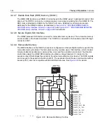
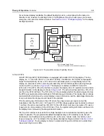
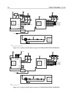
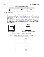
The MMC2 interface on the OMAP processor is configured as a Secure Digital interface used for the
removable memory modules. The removable memory modules use a 10bit interface, which include 4
bit wide bi-directional data bus, command line, clock and three direction control bits. The direction
control bits enable the OMAP SDIO interface to utilize a voltage translator IC, located on the
expansion board that bridges the signals to the actual removable memory device. The SDIO signals
are conveyed to the expansion board via J4001. The expansion board houses a removable memory
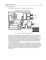
socket (J2101) which is compatible with MicroSD flash devices. See
Figure 3-33
for details.
Figure 3-33.
Removable Memory Outline
Removable Memory
Troubleshooting Diagram
Click on each test point to
see signal
B
d O
l
T
t P i t D
i ti
SDIO
Level
Translator
Voltage
Regulator
OMAP
CPLD
FET
switch
MAKO
EXPANSION BOARD
VOCON BOARD
MPC
MMC2
VSW 3.6
3.0V
VCC 1.875
MMC2_CS0
REMOVABLE
MEMORY CARD
3.0V logic
D3
D2
D1
D0
CMD
MMC2_CMD
MMC2_D3
MMC2_D2
MMC2_D1
MMC2_D0
MMC2_CMD_DIR
MMC2_D1_DIR
MMC2_D0_DIR
MMC2_CLKFB
MMC2_CLK
1.875 Logic
CLK
1
2
3
4
5
16
7
8
9
10
11
12
13
14
15
Note: Signals can only be probed
in Analysis Fixture
6
Содержание ASTRO APX 7000
Страница 1: ......
Страница 4: ...iv Document History Notes ...
Страница 24: ...2 4 Radio Power DC Power Routing VOCON Board Notes ...
Страница 98: ...3 74 Theory of Operation Global Positioning System GPS ...
Страница 104: ...4 6 Troubleshooting Procedures Power Up Self Check Diagnostics and Repair Not for Field Use Notes ...
Страница 163: ...Troubleshooting Charts PA Failure 5 59 ...
Страница 164: ...5 60 Troubleshooting Charts PA Failure ...
Страница 168: ...6 4 Troubleshooting Waveforms Clocks 6 2 2 4 MHz Clock Trace 1 Trace recorded at R6113 Figure 6 2 4 MHz Clock Waveform ...
Страница 174: ...6 10 Troubleshooting Waveforms Audio SSI 6 3 3 Sync Trace 1 Trace recorded at R3005 Figure 6 8 Audio SSI Sync Waveform ...
Страница 175: ...Troubleshooting Waveforms Audio SSI 6 11 6 3 4 BCLK Trace 1 Trace recorded at R3006 Figure 6 9 Audio SSI BCLK Waveform ...
Страница 177: ...Troubleshooting Waveforms RX SSI 6 13 6 4 2 DA Trace 1 Trace recorded at R1005 Figure 6 11 RX SSI DA Waveform ...
Страница 178: ...6 14 Troubleshooting Waveforms RX SSI 6 4 3 FSync Trace 1 Trace recorded at R1004 Figure 6 12 RX SSI FSync Waveform ...
Страница 180: ...6 16 Troubleshooting Waveforms TX SSI 6 5 2 DA Trace 1 Trace recorded at R1017 Figure 6 14 TX SSI DA Waveform ...
Страница 181: ...Troubleshooting Waveforms TX SSI 6 17 6 5 3 FSync Trace 1 Trace recorded at R1007 Figure 6 15 TX SSI FSync Waveform ...
Страница 182: ...6 18 Troubleshooting Waveforms SPI 6 6 SPI 6 6 1 CLK Trace 1 Trace recorded at R6605 Figure 6 16 SPI CLK Waveform ...
Страница 183: ...Troubleshooting Waveforms SPI 6 19 6 6 2 CLK INV Trace 1 Trace recorded at R2325 Figure 6 17 SPI CLK INV Waveform ...
Страница 184: ...6 20 Troubleshooting Waveforms SPI 6 6 3 CS Trace 1 Trace recorded at Pin 34 of J2301 Figure 6 18 SPI CS Waveform ...
Страница 185: ...Troubleshooting Waveforms SPI 6 21 6 6 4 MOSI Trace 1 Trace recorded at R6603 Figure 6 19 SPI MOSI Waveform ...
Страница 187: ...Troubleshooting Waveforms I2C BUS 6 23 6 7 2 SCL 5V Trace 1 Trace recorded at R6204 Figure 6 21 I2C Bus SCA 5V Waveform ...
Страница 188: ...6 24 Troubleshooting Waveforms I2C BUS 6 7 3 SDA Trace 1 Trace recorded at R6209 Figure 6 22 I2C Bus SDA Waveform ...
Страница 194: ...6 30 Troubleshooting Waveforms USB 6 10 2 D Trace 1 Trace recorded at Pin 35 of J3001 Figure 6 28 USB D Waveform ...
Страница 196: ...6 32 Troubleshooting Waveforms UART 6 11 2 TX Trace 1 Trace recorded at F_Boot_Tx Figure 6 30 UART TX Waveform ...
Страница 198: ...6 34 Troubleshooting Waveforms SDRAM 6 12 2 CLKX Trace 1 Trace recorded at TP6308 Figure 6 32 SDRAM CLKX Waveform ...
Страница 276: ...7 58 Troubleshooting Tables List of Board and IC Signals Notes ...
Страница 318: ...8 42 Schematics Boards Overlays and Parts Lists Transceiver RF Boards VHF 700 800 Notes ...
Страница 380: ...8 104 Schematics Boards Overlays and Parts Lists Transceiver RF Boards UHF1 700 800 MHz Notes ...
Страница 432: ...8 156 Schematics Boards Overlays and Parts Lists Transceiver RF Boards UHF1 VHF Notes ...
Страница 458: ...8 182 Schematics Boards Overlays and Parts Lists Transceiver RF Boards UHF1 UHF2 Notes ...
Страница 498: ...8 222 Schematics Boards Overlays and Parts Lists Transceiver RF Boards UHF2 700 800 MHz Notes ...
Страница 546: ...8 270 Schematics Boards Overlays and Parts Lists Transceiver RF Boards UHF2 VHF Notes ...
Страница 606: ...8 330 Schematics Boards Overlays and Parts Lists VOCON Boards Notes ...
Страница 638: ...Glossary 10 Glossary Notes ...
Страница 643: ......


