HC05A24EM USER’S MANUAL
MOTOROLA
1-3
1
1.2
EM LAYOUT
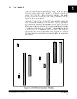
Figure 1-1 shows the layout of the A24EM. Jumper header P4 controls
the path of a target reset. Jumper header P5 can be used to disable the
internal COP of the MCU during software development. Jump header
P6 lets you select the clock-signal source. Jump header P9 selects the
internal oscillator clock divider.
Connectors P7 and P8, for a 56-pin SDIP cable assembly, (purchased
separately from the A24EM.) provide an interface to your target system.
If you install the A24EM in the MMDS05 station module, the target
cable passes through the slit in the station module enclosure. Connector
P1 connects to a logic analyzer. (Connector P1 has more significance for
an EVS system, as an MMDS05 system includes a bus analyzer.)
Expansion header connectors P2 and P3 connect together the EM and
the control board (for an MMDS05) or the EM and the platform board
(for an EVS).
P7
P8
P1
P2
P3
Figure 1-1. HC05A24 Emulator Module
P4
P6
P9
P5
Содержание A24EM
Страница 17: ...HC05A24EM USER S MANUAL MOTOROLA 2 6 2 ...


