HC05A24EM USER’S MANUAL
MOTOROLA
3-3
3
3.1.3
Clock Source Select Header (P6)
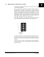
Jumper header P6 determines the source of the clock signal. The dia-
gram below shows the factory configuration: the fabricated jumper
between pins 2 and 3 selects the A24EM canned oscillator clock source.
This is the only correct configuration for an A24EM that is part of an
HC05EVS.
NOTE
The P6 pins 1 and 2 configuration is not correct for an A24EM that is
part of an HC05EVS system.
3.1.4
Clock Divider Header (P9)
Jumper header P9 determines which internal clock divider of the MCU
to use after power on or reset. The diagram below shows the factory con-
figuration: the fabricated jumper between pins 1 and 2 selects the divide
by two MCU clock divider. This is the correct configuration for a 4 MHz
clock source. If a 16 MHz clock source is used. The user must remove
the fabricated jumper between pins 1 and 2 to select the divide by eight
MCU clock divider.
1
2
3
P6
XTAL
MMDS05
FABRICATED
JUMPER
1
2
P9
OPEN = OSC/8
FABRICATED
JUMPER
INTERNAL
CLOCK DIVIDER
CLOSE = OSC/2
Содержание A24EM
Страница 17: ...HC05A24EM USER S MANUAL MOTOROLA 2 6 2 ...


