


Appendix 7
miriac EK-5744 User Manual
V 1.2
52/53
© MicroSys Electronics GmbH 2017
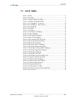
7.3 List of Tables
Table 1-1 Symbols ................................................................................................................. 5
Table 1-2 Conventions ........................................................................................................... 5
Table 2-1 Safety and Handling Precautions ........................................................................... 6
Table 4-1: Component Temperature Ratings ....................................................................... 21
Table 5-1: MCU Pin Mapping – Full Overview ..................................................................... 26
Table 5-2: MCU Pin Mapping – Short Overview ................................................................... 27
Table 5-3: LED Pin Mapping ................................................................................................ 28
Table 5-4: Boot Modes ......................................................................................................... 29
Table 6-1 JTAG Header ....................................................................................................... 31
Table 6-2: JTAG Connector Pin Mapping ............................................................................ 32
Table 6-3: Aurora Pin Mapping ............................................................................................ 33
Table 6-4: Serial Interface Port Mapping .............................................................................. 34
Table 6-5: Ethernet Port Pin Mapping .................................................................................. 35
Table 6-6: CAN Termination Switch State Table .................................................................. 37
Table 6-7: Digital Inputs Electrial Specification .................................................................... 38
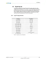
Table 6-8: Digital Inputs Pin Mapping .................................................................................. 39
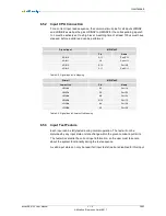
Table 6-9: Digital Inputs Stimulus Pin Mapping .................................................................... 39
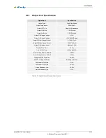
Table 6-10: Digital Output Electrical Specification ................................................................ 41
Table 6-11: Digital Output First Stage Enable Pin Mapping ................................................. 42
Table 6-12. Digital Output Read Back Pin Mapping ............................................................. 43
Table 6-13: Digital Output Pin Mapping ............................................................................... 43
Table 6-14: Digital Output Truth Table ................................................................................. 44
Table 6-15: Digital Outputs First Stage Settling Times ......................................................... 44
Table 6-16: Analog Input 4-20mA Input Validity ................................................................... 45
Table 6-17: Analog Input ADC Pin Mapping ........................................................................ 46
Table 6-18: Analog Input Stimulus Pin Mapping .................................................................. 46
Table 6-19: Analog Input Stimulus Ranges .......................................................................... 47
Table 6-20: Analog Input Settling Time ................................................................................ 47
Table 6-21: Relay Activation Truth Table ............................................................................. 48
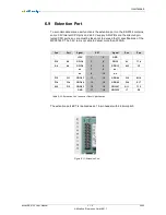
Table 6-22: Extension Port Connector Pinout Specification ................................................. 49
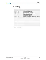
Table 8-1 Document history ................................................................................................. 53


