MicroSys miriac EK5744 Скачать руководство пользователя страница 11


Quick Start Guide 3 


miriac EK-5744 User Manual 

V 1.2 

11/53


© MicroSys Electronics GmbH 2017 


3.3  Operation 


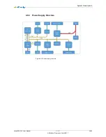
3.3.1  Preinstalled Evaluation Software 

The system is flashed with software, providing the following functionality: 

  Webserver with DHCP support (DHCP capable network needed in order to 

start the demo) 

  Serial console via the RS232 port (115200 Bd, 8N1) 

  CAN loopback test 

  Digital and analog input readout and display at the console 

  Digital outputs can be set via a web browser, just navigate to the unit’s 

assigned IP address at port 80 via HTTP 
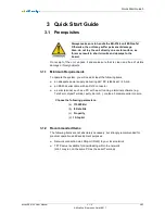
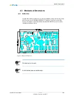
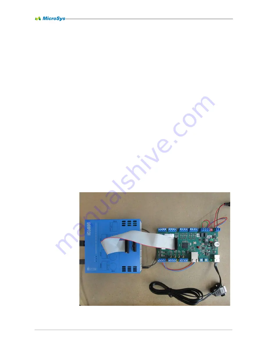
3.3.2  Cabling 


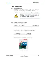
  Connect the 24V power supply to PWR connector on the rear of board 

  Make a connection between PWR and PWIN (picture below shows a red 

and a blue wire) 

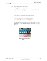
  Make a loopback connection between the 2 CAN ports (picture below 

shows a red and a green wire) 

  Connect RS232 console cable (included) 


Содержание miriac EK5744

Страница 1: ...Creating Embedded Systems miriac EK5744 User Manual V 1 2...

Страница 2: ...Board Views 18 4 7 System Environment 20 4 7 1 Temperature Ratings 20 4 8 Power Supply 22 4 8 1 Input Supply Rating 22 4 8 2 Controller Part Power Connector 22 4 8 3 Digital Output Power Connector 23...

Страница 3: ...issions in this document MicroSys Electronics GmbH neither gives any guarantee nor accepts any liability whatsoever for consequential damages resulting from the use of this manual or its associated pr...

Страница 4: ...d shipment which is dependent on the preferred carrier and the location where you want to have it shipped to by sending a request to MicroSys Electronics GmbH Muehlweg 1 82054 Sauerlach Germany In you...

Страница 5: ...t and its features Table 1 1 Symbols 1 5 2 Conventions Symbol explanation denotes a low active signal denotes the signal flow in the shown direction denotes the signal flow in the shown direction deno...

Страница 6: ...it may become hot during operation Take care not to touch any parts of the circuitry during operation to avoid burns and operate the unit in a well ventilated location Provide an appropriate cooling s...

Страница 7: ...nputs and outputs which have been im plemented following the safety requirements of IEC 61508 and ISO 13849 Single channel architecture is provided for lower safety requirements dual channel archi tec...

Страница 8: ...t 3 4 safe digital outputs 2 safe analog inputs two redundant channels 2 safe digital inputs two redundant channels customized firmware CANopen Safety CIA304 Safety over EtherCAT Profisafe openSAFETY...

Страница 9: ...em you will need at least the following items an adequate power supply delivering 24V DC stabilized 2 A min an RS232 serial cable with an RJ12 connector a serial terminal such as a PC with a port runn...

Страница 10: ...ke sure the switch BOOT located on the EK 5744 carrier board is set properly in order to select the correct boot source and board configuration For more details see chapter 5 3 and 5 4 After Power On...

Страница 11: ...ia the RS232 port 115200 Bd 8N1 CAN loopback test Digital and analog input readout and display at the console Digital outputs can be set via a web browser just navigate to the unit s assigned IP addre...

Страница 12: ...tack Started DHCP service Mounted FileSystem HTTP Server Initiated Waiting for DHCP server to assign IP DHCP assigned IP 192 168 0 191 WebServer is accessible via web browser Use the assigned IP as UR...

Страница 13: ...System Description 4 miriac EK 5744 User Manual V 1 2 13 53 MicroSys Electronics GmbH 2017 4 System Description This section describes all parts of the EK 5744 system 4 1 Block Diagram EK 5744...

Страница 14: ...Switches Push button Switch Push button Switch DIP Switch DIP Switch 2 pin Header 2 pin Header Power On Reset Soft Reset BMOD Boot Mode CAN1 2 Termination On Off Power Down Debug Board Connectors Cont...

Страница 15: ...B is suitable for use with an installation component housing of the BC161 series from PHOENIX CONTACT Therefore there are no mounting holes on the board It complies with the standard DIN 43880 for use...

Страница 16: ...System Description 4 miriac EK 5744 User Manual V 1 2 16 53 MicroSys Electronics GmbH 2017 4 4 Board Layout Figure 4 2 Board Layout Top Side...

Страница 17: ...System Description 4 miriac EK 5744 User Manual V 1 2 17 53 MicroSys Electronics GmbH 2017 Figure 4 3 Board Layout Bottom Side...

Страница 18: ...miriac EK 5744 User Manual V 1 2 18 53 MicroSys Electronics GmbH 2017 4 6 Board Views Figure 4 4 Board Front Side View Figure 4 5 Board Rear View Figure 4 7 Board Left Hand Side View Figure 4 6 Board...

Страница 19: ...System Description 4 miriac EK 5744 User Manual V 1 2 19 53 MicroSys Electronics GmbH 2017 Figure 4 9 Board Top View Figure 4 8 Board Bottom View...

Страница 20: ...X5R 55 C 85 C C 1206 XXX X7R 55 C 125 C C 1206 XXX X5R 55 C 85 C C 1210 XXX X7R 55 C 125 C C 1210 XXX X5R 55 C 125 C C 2220 XXX X7R 55 C 125 C C EEVFK1J221Q 40 C 105 C D 1PS70SB20 55 C 125 C D BAS70L...

Страница 21: ...C 155 C R 2512 XXXX 65 C 170 C RY FIN 30 22 7 024 40 C 850 C ST FCI 61885 40 C 70 C ST SAM ASP 137973 01 55 C 125 C ST WE 691 101 710 002 40 C 105 C SW KNITTER TSE8S 1 40 C 85 C SW TYCO 1571983 4 30...

Страница 22: ...ng polarity and over current DO NOT exceed the rated maximum values for the power supply This may result in severe permanent damage to the unit as well as possible serious injury 4 8 2 Controller Part...

Страница 23: ...erating Range 24V DC 5 min 1A Power is fed to the IO unit via the 2 pin pressure clamp PWIN Manufacturer W rth Elektronik Type 691 101 710 002 Mates with 1 2mm wire The red power indicator led is acti...

Страница 24: ...System Description 4 miriac EK 5744 User Manual V 1 2 24 53 MicroSys Electronics GmbH 2017 4 8 4 Power Supply Structure Figure 4 12 Power supply structure...

Страница 25: ...ion a3 DOUT0 Output Data high non inverted output pin state a5 LDINB Output Stimulus low global for all digital inputs a11 DIN0 Input Data low inverted input pin state a14 HAIN7 Output Stimulus low un...

Страница 26: ...Stimulus low unique for this digital input m15 HAIN1 Output Stimulus low unique for this analog input n15 HDIN3 Output Stimulus low unique for this digital input p5 HDIN1 Output Stimulus low unique fo...

Страница 27: ...h14 AU TX0P r2 SBC IO2 b14 PWENA h15 JTMS r4 RMII RXDV b15 DPWSTD h17 JTCK r5 AIN1 c1 DPWSTA j14 AU TX0N r6 AIN3 c2 DPWSTC j15 AU CLKN r10 DOSTA1 c4 SBC IO3 j17 JTDI r11 DOSTA2 c5 GPIO13 k1 JNRDY r12...

Страница 28: ...e LD2 yellow output 1 active output 1 inactive digital output driver state LD3 yellow output 2 active output 2 inactive digital output driver state LD4 yellow output 3 active output 3 inactive digital...

Страница 29: ...le FAB ABS1 ABS0 USER Boot ID Mode SW1 SW2 SW3 SW4 OFF ON ON Serial Boot SCI OFF ON OFF Serial Boot CAN ON Valid Single Chip ON Not found Static Mode Table 5 4 Boot Modes Switch 4 of the DIP switch is...

Страница 30: ...e jumper PWON connects the input IO_0 of the MC33907 power controller to its input voltage to activate the SBC The jumper DBUG is used to enter the Debug mode of the SBC In Debug mode any errors from...

Страница 31: ...ovides all standard JTAG signals for an ARM interface on a 2x5 pin header Pin 7 of this header usually connects the return clock RTCK and is not used on the EK 5744 For boundary scan purposes it can b...

Страница 32: ...LVTTL Input 8 PORST D6 EXT_POR_B LVTTL IO 10K Pullup 9 RESET P2 RESET_B LVTTL IO 10K Pullup 10 JTMS H15 TMS LVTTL Input 11 3 3V Output 12 GND 13 JNRDY K1 Port J9 LVTTL 14 JCOMP A6 JCOMP LVTTL Input 1...

Страница 33: ...Port B5 LVTTL Input 9 AU TX1N K14 Port G15 LVDS Output 10 JTDO G14 Port B4 LVTTL Output 11 GND Output 12 JCOMP A6 JCOMP LVTTL Input 10K Pulldown 13 n c 14 n c 15 n c 16 JNEVTI L2 Port F11 LVTTL Input...

Страница 34: ...works with 115200 Baud and no flow control 6 2 1 RJ11 Connector LIN Manufacturer FCI Type 61885 Mates with Standard RJ11 jack 6 2 2 LIN Connector Pinout JTAG MPC5744P I O Level Description Pin Signal...

Страница 35: ...r4 RMII RXDV D7 receive data valid t3 RMII RXER I1 receive error a10 MINT I3 interrupt b6 RMII MDCK F0 management clock f2 RMII MDIO H7 management data m17 RMII TXEN G5 transmit enable n14 RMII CLK G8...

Страница 36: ...CAN interfaces CAN1 and CAN2 are accessible via two 2 terminal wire connectors The necessary 120 Ohm end point termination can be activated by two DIP switches 6 4 1 CAN Connector Block Manufacturer...

Страница 37: ...is activated if the corresponding DIP switch is set to ON Manufacturer W rth Elektronik Type 418117270902 Setting TERM 1 TERM 2 CAN1 CAN2 OFF OFF no termination no termination ON OFF 120R termination...

Страница 38: ...put is fully testable during operation and has the following specifications A valid input can only be read by the CPU if all test features of the input are disabled 6 5 1 Input Port Specification Digi...

Страница 39: ...2 B13 Port H9 XDIN3 P17 Port D11 Table 6 8 Digital Inputs Pin Mapping Stimuli MPC5744P Low active Pin Name HDIN0 K4 Port I8 HDIN1 P5 Port I12 HDIN2 M3 Port I10 HDIN3 N15 Port I5 LDINA B4 Port D2 LDINB...

Страница 40: ...ssible due to a shorted output driver the output power for all four switches can be cut off To enable one of the first stage switches stage AB or stage CD both PWEN lines must be set to low The states...

Страница 41: ...V Output On Range Voltage 23V 24V Supply Output Off Low Range Current 0 14V 0 1mA Output Off High Range Current 14 24V 10mA Output On Range Current Nominal 0 25A Turn On Rise Time 25ns Turn Off Fall T...

Страница 42: ...oad switch has a delay of 250us which must be taken into account for the status verification For testing the first stage without disturbing active outputs the following sequence must be performed We a...

Страница 43: ...undershots from inductive loads There are two redundant status line read back circuits for each output which reflect the real state on the output connector no matter if the output driver is active or...

Страница 44: ...0 1 1 0 0 1 0 on Out2 ON 0 0 1 1 0 0 0 1 on Out3 ON 1 1 0 1 X X X X off all off 1 1 1 0 X X X X off all off 1 1 0 0 0 0 0 0 on all off 0 0 0 0 0 0 0 0 on all off 1 1 0 0 1 0 0 0 on Out0 ON 1 1 0 0 0 1...

Страница 45: ...ignals HAIN0 to HAIN7 as well as LAIN must all be at a logical high The range of 0 20mA at the connector is translated to an analog voltage of 0V to 2 9V at the MPC5744P port pin according to the foll...

Страница 46: ...hin the nominal range will be overwitten by any active stimulus Connector MPC 5744P Name Signal Signal Pad Port ANI0 XAIN01 AIN0 U7 ADC0_AN0 AIN1 R5 ADC0_ADC1__AN11 ANI1 XANI23 AIN2 U10 ADC1_AN7_ADC3_...

Страница 47: ...The influence of an external injected current is below 1mV 6 7 1 4 Analog Settling Times The analog input circuitry is realized with a low pass filter The settling time of this filter and the stimuli...

Страница 48: ...as well with AC as with DC voltages The relay can only be activated by the SBC and the CPU Therefore the two lines MCU FSO and SBC FSO must be set active The SBC FSO is derived from the MC33907 pin FS...

Страница 49: ...e IO specifications of the MPC5744P The 3 3V rail is not able to deliver more than 250mA The extention port EXT is realized as an 18 pin header with 2 54mm pitch Pad Port Signal EXT Signal Port Pad 3...

Страница 50: ...the document note that this list does not claim to be complete or exhaustive ARM Advanced RISC Machine ESD Electrostatic Discharge GND Ground GPIO General Purpose IO GPL General Public License JTAG J...

Страница 51: ...ector 22 Figure 4 11 Digital Output Power Connector PWIN 23 Figure 4 12 Power supply structure 24 Figure 5 1 Processor Block diagram 25 Figure 5 2 LED Location and Numbering 28 Figure 5 3 MPX LEDs 28...

Страница 52: ...ble 6 7 Digital Inputs Electrial Specification 38 Table 6 8 Digital Inputs Pin Mapping 39 Table 6 9 Digital Inputs Stimulus Pin Mapping 39 Table 6 10 Digital Output Electrical Specification 41 Table 6...

Страница 53: ...al Release Version preliminary 2017 08 01 1 01 MIPI Chapter and Rev 2 photos added 2017 09 01 1 1 Some review inputs implemented Typos corrected Default setting for switches marked Preliminary waterma...

Отзывы: