9
SY87729/39L
Evaluation Board
Micrel, Inc.
M9999-071906
[email protected] or (408) 955-1690
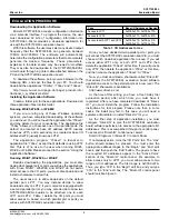
The status line will have a different message if there
were no errors in the configuration. For example, starting
with the download application looking like Figure 17, if you
click the “Download” button, you should end up with the
download application looking like Figure 18. Note that the
status line says “Configuration Sent”. Unless these two words
appear in the status line after selecting the “Download”
button, the configuration was not sent due to some error.
For those users who have two SY87729/39L evaluation
boards connected to LPT1 and LPT2, you must sometimes
swap which parallel port to download to. In the system
menu, there is an item labeled “Swap I/O." Selecting this
menu item switches between LPT1 and LPT2. The title bar
changes to indicate which parallel port is currently active.
A title bar like in Figure 16, that just says “739ev," indicates
that LPT1 is being used for downloads. If the title bar says
“739ev - LPT2," then LPT2 is being used for downloads.
Please note that, if using “Direct-IO”, and if it’s not configured
to allow I/O access to both parallel ports, selecting LPT2
will cause the program to be terminated by the operating
system.
Using an External Signal Generator and Measuring
Frequency Output
Now we will delve into the hardware aspects of the
SY87729/39L evaluation board, and assume that you have
installed and configured the applications, and are somewhat
familiar with them.
This section describes how to set up a test configuration
similar to that in Figure 1, where an external clock source
feeds the SY87729/39L evaluation board, and a frequency
counter verifies the resultant output. You will need:
■
A power supply
■
A frequency counter
■
A signal generator
■
A 50
Ω
termination SMA
■
A SY87729/39L evaluation board
■
A PC with the evaluation software installed
■
A printer cable
The following steps allow the user to verify frequency of
operation of the SY87729/39L evaluation board:
1.
Connect Power Source: The power supply should be
set to about 3.3V. Current consumption will be between
250mA and 300mA. Connect the positive power supply to
the red or yellow banana jack, J1, labeled “V
CC
” under it on
the silk screen. Connect the negative power supply to the
black banana jack, J2, labeled “GND” under it on the silk
screen.
2.
Connect Clock Source: Set your clock source to
generate LVPECL level signals at the input frequency of
interest. For LVPECL, the voltages are referenced to V
CC
,
so the voltage to set the signal generator to depends on the
value of V
CC
. For a V
CC
of 3.3V, the high level of the clock
signal should be between 2.135V and 2.42V. The low level
of the clock signal should be between 1.49V and 1.825V.
Set the high and low levels to something like 2.3V and
1.6V. The frequency should be in the tens of Mega-Hertz.
Connect this clock source to and REFCLK– (J3
and J4) via SMA patch cables.
The SY87729/39L evaluation board is meant to be run
with a differential clock input. Though we don’t recommend
it, you may feed a single-ended PECL clock on one input,
and bias the other input, via a power supply, to about 2.0V.
Expect a more jittery output clock in this case.
In the set up in Figure 1, an HP8133A signal source
generates the clock. The clock frequency was chosen to be
25MHz. Since the 8133A only goes down to 32MHz, the
frequency was set to 100MHz with a post-divide of 4. In
addition, since the 8133A’s edges are very fast, the clock
output edges were slowed down with a pair of 2000ps
transition time converters (HP15438A), one on each of the
complementary outputs of the 8133A.
3.
Connect Configuration Source: Attach the printer cable
between the PC parallel port and the SY87729/39L
evaluation board’s Centronics plug, J9. Launch the download
software and verify that either the message “729 Locked,"
“729 NOT Locked” or “739 Locked," “739 NOT Locked”
appears at the upper right of the download application
window.
4.
Configure the SY87729/39L Evaluation Board: Launch
a calculation module, and set the “Reference” edit box to
the frequency of the clock source. Enter the target frequency
in the “729 Output” or “739 Output” edit box and have the
calculation module determine the configuration parameters.
Have the download module configure the SY87729/39L
evaluation board, and verify that the indicator at the upper
right of the download application is green, and that it says
“729 Locked” or “739 Locked."
5.
Verify Output Frequency: Connect a frequency counter,
capable of measuring the expected output frequency, and
terminating into 50
Ω
, to , J5, via an SMA patch
cable. Connect a 50
Ω
termination to CLKOUT–, J6. Verify
that the frequency counter indicates the expected output
frequency.
Using the Supplied Reference Oscillator and Measuring
Jitter
This section describes how to set up the test configuration
in Figure 2, where the SY87729/39L evaluation board’s
internal clock source is used, and the output jitter is
measured. You will need:
■
A power supply
■
A TIA (Time Interval Analyzer)
■
Two 1-foot long SMA patch cables, length matched
■
A 50
Ω
termination SMA
■
A SY87729/39L evaluation board
■
A PC with the evaluation software installed
■
A printer cable


