Rev 1.4
Mellanox Technologies
44
Appendix C: Interface Connector Pinouts
C.1
SFP+ Interface
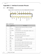
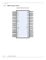
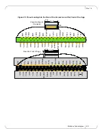
Figure 25: SFP+ Connector Pinout - Rear View of Module With Pin Placement
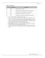
Table 13 - SFP+ Pinout
Pin
Symbol Name
Description
1
VeeT
Transmitter Ground (Common with Receiver Ground)
a
2
TX_Fault
Transmitter Fault.
b
3
TX_Disable
Transmitter Disable. Laser output disabled on high or open.
c
4
SDA
2-wire Serial Interface Data Line
d
5
SCL
2-wire Serial Interface Clock Line
d
6
MOD_ABS
Module Absent. Grounded within the module
d
7
RS0
No connection required
8
RX_LOS
Loss of Signal indication. Logic 0 indicates normal operation.
e
9
RS1
No connection required
10 VeeR
Receiver Ground (Common with Transmitter Ground)
a
11 VeeR
Receiver Ground (Common with Transmitter Ground)
a
12
RD-
Receiver Inverted DATA out. AC Coupled
13
RD+
Receiver Non-inverted DATA out. AC Coupled
14
VeeR
Receiver Ground (Common with Transmitter Ground)
a
15
VccR
Receiver Power Supply
V
eeT
V
eeT
V
eeT
T
X
_F
au
lt
T
X
_D
is
abl
e
SD
A
SC
L
MO
D
_
A
B
S
RS
0
RX
_L
O
S
RS
1
Ve
eR
V
eeR
Vee
R
VccT
Vcc
R
TD
+
TD-
RD
-
RD+
1
2
3
4
5
6
7
8
9
1
2
3
4
5
6
7
8
9
0
1
1
1
1
1
1
1
1
1
2
10


