background image

the slave address. Next follows a number of data
bytes. The slave returns an acknowledge bit after
each received byte. Data is transferred with the most
significant bit (MSB) first.

Data transfer from a slave transmitter to a master
receiver. 

The first byte (the slave address) is trans-

mitted by the master. The slave then returns an
acknowledge bit. Next follows a number of data
bytes transmitted by the slave to the master. The
master returns an acknowledge bit after all received

bytes other than the last byte. At the end of the last
received byte, a not acknowledge is returned.

The master device generates all the serial clock puls-
es and the START and STOP conditions. A transfer is
ended with a STOP condition or with a repeated
START condition. Since a repeated START condition
is also the beginning of the next serial transfer, the
bus will not be released. Data is transferred with the
most significant bit (MSB) first.

DS3232

Extremely Accurate I

2

C RTC with 

Integrated Crystal and SRAM

____________________________________________________________________

17

...

A

XXXXXXXX

A

1101000

S

0

XXXXXXXX

A

XXXXXXXX

A

XXXXXXXX

A

P

<R/W>     <WORD ADDRESS (n)>                    <DATA (n)>                          <DATA (n + 1)>                              <DATA (n + X)

S - START
A - ACKNOWLEDGE (ACK)
P - STOP
R/W - READ/WRITE OR DIRECTION BIT ADDRESS

DATA TRANSFERRED

(X + 1 BYTES + ACKNOWLEDGE)

MASTER TO SLAVE

SLAVE TO MASTER

<SLAVE

ADDRESS> 

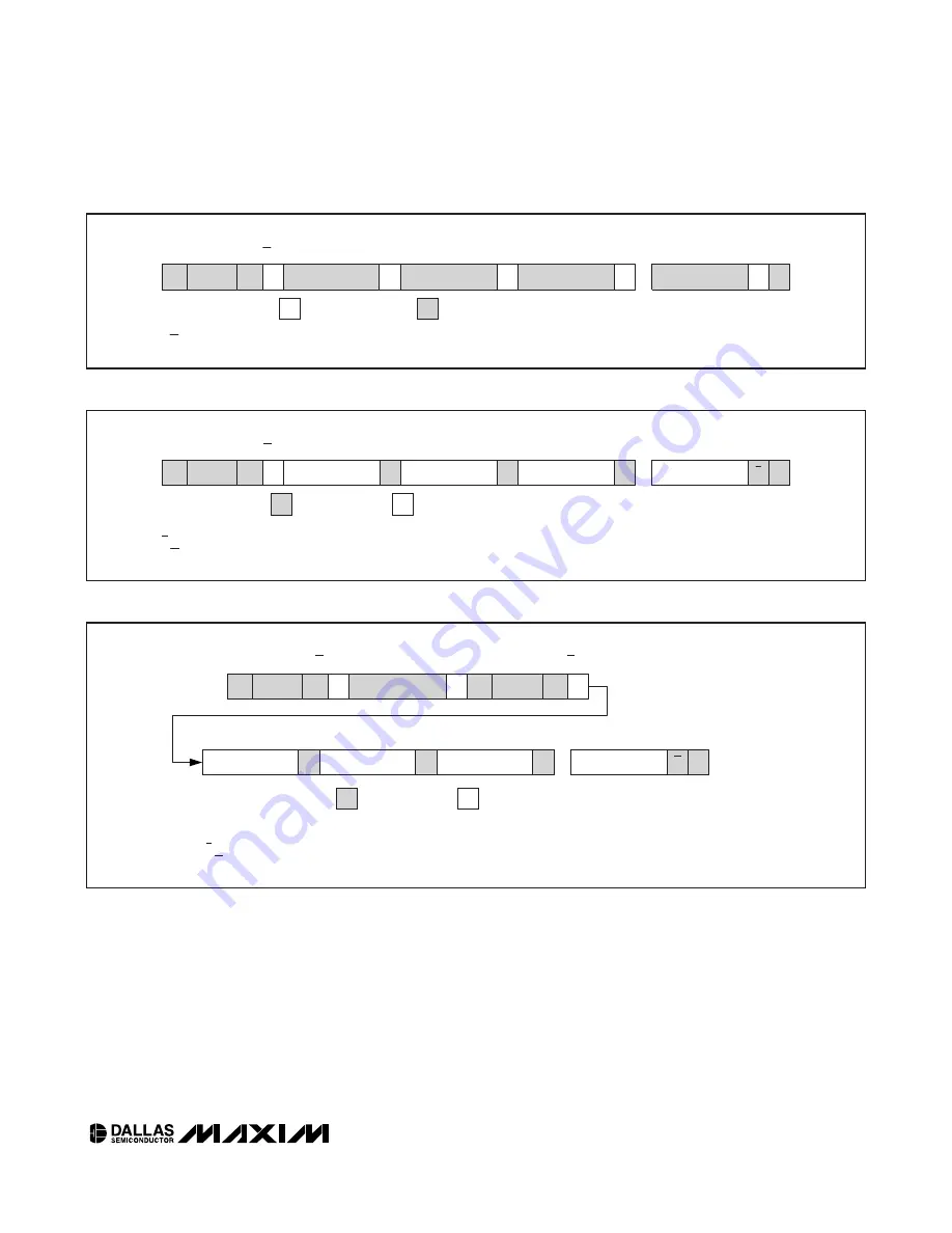
Figure 3. Data Write—Slave Receiver Mode

...

A

XXXXXXXX

A

1101000

S

1

XXXXXXXX

A

XXXXXXXX

A

XXXXXXXX

A

P

S - START
A - ACKNOWLEDGE (ACK)
P - STOP
A - NOT ACKNOWLEDGE (NACK)
R/W - READ/WRITE OR DIRECTION BIT ADDRESS

DATA TRANSFERRED

(X + 1 BYTES + ACKNOWLEDGE)

NOTE: LAST DATA BYTE IS FOLLOWED BY A NACK.

MASTER TO SLAVE

SLAVE TO MASTER

<R/W>             <DATA (n)>                           <DATA (n + 1)>                       <DATA (n + 2)>                             <DATA (n + X)>    

<SLAVE

ADDRESS>

Figure 4. Data Read—Slave Transmitter Mode

S - START
Sr - REPEATED START
A - ACKNOWLEDGE (ACK)
P - STOP
A - NOT ACKNOWLEDGE (NACK)
R/W - READ/WRITE OR DIRECTION BIT ADDRESS

<R/W>

<WORD ADDRESS (n)>

<SLAVE ADDRESS (n)>

<SLAVE

ADDRESS>

<R/W>

A

XXXXXXXX

A

1101000

1101000

S

Sr

0

A

1

DATA TRANSFERRED

(X + 1 BYTES + ACKNOWLEDGE)

NOTE: LAST DATA BYTE IS FOLLOWED BY A NACK.

MASTER TO SLAVE

SLAVE TO MASTER

A

XXXXXXXX

XXXXXXXX

A

XXXXXXXX

A

XXXXXXXX

A

P

 <DATA (n)>                        <DATA (n + 1)>                       <DATA (n + 2)>                             <DATA (n + X)>

...

Figure 5. Data Write/Read (Write Pointer, Then Read)—Slave Receive and Transmit

Содержание Maxim DS3232 Series

Страница 1: ...atures Accuracy 2ppm from 0 C to 40 C Accuracy 3 5ppm from 40 C to 85 C Battery Backup Input for Continuous Timekeeping Operating Temperature Ranges Commercial 0 C to 70 C Industrial 40 C to 85 C 236...

Страница 2: ...ard Layout and Assembly section PARAMETER SYMBOL CONDITIONS MIN TYP MAX UNITS VCC 2 3 3 3 5 5 Supply Voltage VBAT 2 3 3 0 5 5 V Logic 1 Input SDA SCL VIH 0 7 x VCC VCC 0 3 V Logic 0 Input SDA SCL VIL...

Страница 3: ...63 31 69 0 C to 40 C 2 2 Frequency Stability vs Temperature f fOUT VCC 3 3V or VBAT 3 3V 40 C to 0 C and 40 C to 85 C 3 5 3 5 ppm Frequency Stability vs Voltage f V VCC 3 3V or VBAT 3 3V 1 ppm V 40 C...

Страница 4: ...de 100 Data Setup Time Note 10 tSU DAT Standard mode 250 ns Fast mode 0 6 Start Setup Time tSU STA Standard mode 4 7 s Fast mode 300 Rise Time of Both SDA and SCL Signals Note 11 tR Standard mode 20 0...

Страница 5: ...te I2C RTC with Integrated Crystal and SRAM _____________________________________________________________________ 5 Pushbutton Reset Timing tRST PBDB RST Power Switch Timing VCC VPF MAX RST VPF MIN tV...

Страница 6: ...of the falling edge of SCL Note 9 The maximum tHD DAT needs only to be met if the device does not stretch the low period tLOW of the SCL signal Note 10 A fast mode device can be used in a standard mod...

Страница 7: ...DS3232 toc03 TEMPERATURE C SUPPLY CURRENT A 80 60 40 20 0 20 0 700 0 800 0 900 0 600 40 VCC 0V BB32kHz 0 VBAT 3 4V VBAT 3 0V FREQUENCY DEVIATION vs TEMPERATURE vs AGING DS3232 toc04 TEMPERATURE C FREQ...

Страница 8: ...and accurate reference clock and maintains the RTC to within 2 minutes per year accu racy from 40 C to 85 C The TCXO frequency output is available at the 32kHz pin The RTC is a low power clock calend...

Страница 9: ...t When using the device with the VBAT input as the primary power source this pin should be decoupled using a 0 1 F to 1 0 F low leakage capacitor When using the device with the VBAT input as the backu...

Страница 10: ...ising edge Upon detecting release the DS3232 forces the RST pin low and holds it low for tRST The same pin RST is used to indicate a power fail con dition When VCC is lower than VPF an internal power...

Страница 11: ...RAM ____________________________________________________________________ 11 Figure 1 Address Map for DS3232 Timekeeping Registers and SRAM Note Unless otherwise specified the registers state is not de...

Страница 12: ...ch of the time of day date alarm registers are mask bits Table 2 When all the mask bits for each alarm are logic 0 an alarm only occurs when the values in the timekeeping registers match the correspon...

Страница 13: ...e bits control the frequency of the square wave output when the square wave has been enabled The following table shows the square wave frequencies that can be select ed with the RS bits These bits are...

Страница 14: ...Output EN32kHz This bit indi cates the status of the 32kHz pin When set to logic 1 the 32kHz pin is enabled and outputs a 32 768kHz square wave signal When set to logic 0 the 32kHz pin goes low The in...

Страница 15: ...s section for a graph showing the effect of the register on accu racy over temperature Temperature Registers 11h 12h Temperature is represented as a 10 bit code with a res olution of 0 25 C and is acc...

Страница 16: ...clock signal The data on the line must be changed during the low period of the clock signal There is one clock pulse per bit of data Each data transfer is initiated with a START condition and terminat...

Страница 17: ...___________________________________________________ 17 A XXXXXXXX A 1101000 S 0 XXXXXXXX A XXXXXXXX A XXXXXXXX A P R W WORD ADDRESS n DATA n DATA n 1 DATA n X S START A ACKNOWLEDGE ACK P STOP R W READ...

Страница 18: ...are after reception of the slave address and direction bit The slave address byte is the first byte received after the master generates a START condition The slave address byte contains the 7 bit DS32...

Страница 19: ...ower is applied and the oscillator is disabled 9 Added a paragraph to the Pushbutton Reset Function section about how the RST output operation does not affect the device s internal operation 10 3 10 0...

Отзывы: