background image

2. Factory Initialization Mode

Initialize backup data of the MCU.

2.1. Starting up

1. Press the power operation button to turn off the power, and remove the AC plug from the socket.

2. Insert the AC plug while pressing buttons "

INPUT

" and "

BACK

" together, and wait for more than 3 

seconds.

3. Release buttons "

INPUT

" and "

BACK

" when the power indicator turns green.

4. All lights on the display illuminate for 2 seconds.  The power indicator lights up in orange.

5. All lights on the display turn off for 2 seconds.

6. All of the indicators illuminate for 4 seconds.

7. "

Factory Reset

" is shown on the display for 5 seconds.

    The settings for the Installer Setup is also initialized.

    Network function settings are not initialized.

2.2. Factory Reset item

Items

Default

INPUT

Internet Radio

Dimmer

100%

Sleep

Off

Repeat / Random / Program

Off

Setup Menu items

Clear all

Variable Volume

54 (-40dB)

Favorites list

Clear

Standby / Power On

Power On

Protection history

Delete

Update retry flag

Clear

3. All Device USB Update

Perform an update by USB memory.

The firmware of all devices in the unit is forcibly updated without performing a version check.

Button and remote control operation is not recognized during the update.

Insert the AC plug while pressing buttons "

INPUT

" and "

ENTER

" together, and wait for more than 3 

seconds.

•  "

All Device USB Update

" is displayed for 5 seconds.

The display during this update is the same as standard update mode.

4. Firmware Factory Restore

Used when replacing the Network module.

See "

3. Update method when the MAIN PCB or network module is replaced (Using a USB flash drive 

U3001, U3013, NETWORK MODULE)

"

5. Network Function Reset

Initializes network settings.

5.1. Actions

The following items are initialized.

(1)  Network setup

(2)  Friendly Name

(3)  Auto Update setting

(4)  Allow Update setting

(5)  Time Zone setting

(6)  Queue list

(7)  Internet Radio recently played station

(8)  Quick Select playback station

(9)  AirPlay Password

(10) Bluetooth Pairing History

(11) Crestron Connected Setup

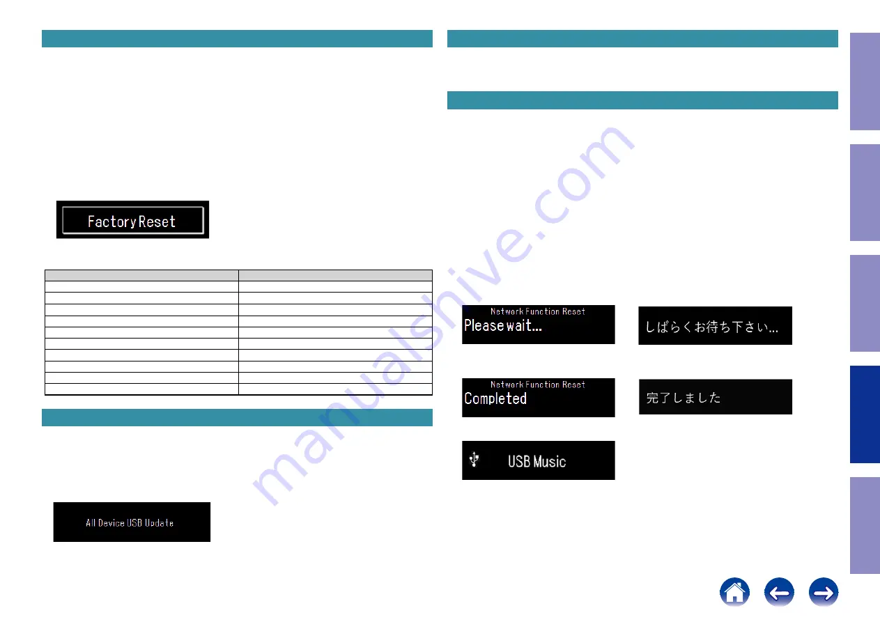
5.2. Starting up

While the power is on, hold down buttons "

POWER

" and "

BACK

" for at least 3 seconds.

(1)  "

Please wait

" is displayed.

    Changes between ".", then ".." and "..." for 1 second each.

                (English is selected) 


(Japanese is selected)

(2)  "

Completed

" is shown on the display for 5 seconds.

                (English is selected) 


(Japanese is selected)

(3)  This is displayed for 5 seconds before returning to the normal display.

Before Servicing 

This Unit

Electrical

Mechanical

Repair Information

Updating

58

Содержание NA6006

Страница 1: ...m NA6006 AP ZH index php JP http manuals marantz com NA6006 JP JA index php Upload is planned for the time of a future press release BEFORE SERVICING THIS UNIT ELECTRICAL MECHANICAL REPAIR INFORMATION UPDATING Service Manual Ver 1 For purposes of improvement specifications and design are subject to change without notice Please use this service manual when referring to the operating instructions wi...

Страница 2: ...AND OPTICS ONLINE PARTS LIST Accessing the Parts List Searching Part Numbers or Ref Numbers NOTE FOR PARTS LIST SERIAL NUMBER Serial Number Organization SKU Code of this Unit POST SERVICE PRECAUTIONS Initializing this Unit Before Servicing This Unit Electrical Mechanical Repair Information Updating 2 ...

Страница 3: ...c diagrams and parts lists be sure to use the designated parts Be sure to mount parts and arrange the wires as they were originally placed For safety seasons some parts use tapes tubes or other insulating materials and some parts are mount ed away from the surface of printed circuit boards Care should also be taken with the positions of the wires by arranging them and using clamps to keep them awa...

Страница 4: ...PUT CONDITION 4 CIRCUIT AND PARTS ARE SUBJECT TO CHANGE WITHOUT PRIOR NOTICE Electrostatic breakdown of the semi conductors or optical pickup may occur due to a potential differ ence caused by electrostatic charge during unpacking or repair work 1 Ground for Human Body Be sure to wear a grounding band 1 M ohm that is properly grounded to remove any static electricity that may be charged on the bod...

Страница 5: ...mbers or Ref numbers 1 Enter the part number or Ref number in the search window of the Parts List and press the search button 2 The search results are displayed The name of the sheet in which the search part is used and the part s line are displayed 3 Next click the Sheet section of the search results 1 Parts indicated by nsp on this table cannot be supplied 2 When ordering a part make a clear dis...

Страница 6: ...nization The 14 digit serial number that contains the code of the manufacturing plant and the manufacturing date SKU code 14 digits Factory code Cumulative serial number Manufactured Year month The last 2digit of year Month 01 12 SKU Code of this Unit Before Servicing This Unit Electrical Mechanical Repair Information Updating 6 ...

Страница 7: ...ializing the device restores the customized settings to the factory settings Write down your settings in advance and reconfigure the settings after initialization Use network initialization mode to initialize the network related settings 1 Press the power operation button to turn off the power and remove the AC plug from the socket 2 Insert the AC plug while pressing button POWER and wait for more...

Страница 8: ...8 POWER SCH09 SMPS PRINTED CIRCUIT BOARDS FRONT HEADPHONE POWER SW WI FI ANT L GUIDE WI FI ANT R GUIDE FFC GUIDE POWER AUDIO MAIN SMPS BLOCK DIAGRAM POWER DIAGRAM WIRING DIAGRAM SEMICONDUCTORS 1 IC s 2 OLED DISPLAY 3 Remote Code Table Before Servicing This Unit Electrical Mechanical Repair Information Updating 8 ...

Страница 9: ...N K C3045 C3050 100 6 3 RV3 C3051 100 6 3 RV3 4 7UF K 1608 C3052 R3034 OPEN 27K OPEN R3030 OPEN 1608 OPEN OPEN 1608 R3033 TO PLD SHEET TO DIR SHEET 4 7UF K 1608 C3061 100N K C3063 IOEXP_ INT R3045 33 R3041 4K7 100N K C3069 30P J C3071 30P J C3074 10K R3074 1N K C3072 IOEXP_ INT 33 R3098 S_FLASH_SO R3085 0 GND_D 33 R3107 33 R3108 10N K C3232 TO PLD SHEET TO PLD SHEET TO FRONT B D 1 19 17 15 7 9 11 ...

Страница 10: ...08 C3131 C3130 1N K C3139 1500P 1608 4 7UF K 1608 C3140 4 7UF K 1608 C3142 0 R3196 OPEN R3230 OPEN C3160 C3163 47 16 RV3 100N K C3164 1 8 3 6 2 4 5 7 TC7WHU04FU TRB U3011 10U K 2012 C3165 OPTICAL OUT DIR R3191 OPEN 1608 OPTICAL IN BACK PANEL DIR2_PLD_PBCK DIR2_PLD_LRCK DIR2_PLD_MCK ADC_PLD_DATA DIR1_PLD_DATA ADC_PLD_PBCK DIR1_PLD_PBCK DIR1_PLD_SPDIF PLD_DAC2_DSDR3 PLD_DAC2_DSDL4 PLD_DAC2_DATA3 DSD...

Страница 11: ..._TDM_FS_SL T15 33 R3308 1K R3310 R3307 OPEN 33 R3312 33 R3313 33 R3315 PLD_DAC1_MCK OPEN R3317 10K R3319 10K R3320 1K R3321 HP_GAIN_M DAC_CLK_SEL I2C_SDA_DAC1 DAC1_MUTE TMS TDO TCK I2C_SCL_CS2K DAC_I2C_DATA DAC_CLK_SEL HP_GAIN_M DAC_GPIO MUTE GND_D GND_D GND_D GND_D GND_D TO DIR SHEET AK4458 100N K C3170 4 7UF K 1608 C3169 100N K C3172 4 7UF K 1608 C3173 100N K C3176 R3256 100 R3246 33 100N K C318...

Страница 12: ...C3226 100N K 33 R3442 33 R3445 33 R3443 33 R3449 33 R3448 33 R3446 33 R3451 TO CPU SHEET 79 75 71 67 63 59 55 51 49 47 45 43 41 37 33 29 25 21 17 13 9 7 5 3 80 76 72 68 64 60 56 52 50 48 46 44 42 38 34 30 26 22 18 14 10 8 6 4 77 73 69 65 61 57 53 39 35 31 27 23 19 15 11 1 78 74 70 66 62 58 54 40 36 32 28 24 20 16 12 2 SM2532CV 2X40 CN3010 AIOS4_WAKEUP AIOS4_STBY_STATUS NET5V_POWER NET3V3_POWER NET...

Страница 13: ...3K AX R2089 560 AX Q2020 2N5401S Q2031 2N5401S R2104 470 AX Q2035 2N5401S 33K AX R2093 Q2041 2SA1312 B R2120 10 AX 470 AX R2097 R2105 82 AX 82 AX R2108 R2122 47 AX R2123 10K AX R2127 10K AX INC2002AC1 Q2048 C2045 100P C2049 1N K INC2002AC1 Q2050 C2051 OPEN C2047 OPEN BKT2001 TO MAIN B D TO POWER B D C2092 220 25 ROA PCMDATA DSDR SPDIF DIR_MCK LEGO CLK HP_GAIN_H HP_ON OFF RCH_OUT LCH_OUT GND_A A_MU...

Страница 14: ...608 R2357 0 1608 R2359 0 1608 R2256 0 1608 R2258 R2148 100K R2149 100K 10K R2237 D2034 LBAS16HT1G 2012 LOUT GND_HP HP_DET ROUT GND_HP 100K R2193 R2181 33 AX R2180 33 AX R2152 5K6 AX R2155 5K6 AX R2156 5K6 AX R2159 5K6 AX 220 16 RA2 C2055 C2056 220 16 RA2 R2164 47 AX R2167 47 AX R2168 47 AX R2171 47 AX L2002 CB05YTYH221 2012 L2003 CB05YTYH221 2012 C2061 100 25 RFO HP_GAIN_M HP_ON OFF HP_DET GND_A L...

Страница 15: ...04 S103 R434 1K5 R435 1K8 RIGHT KEY2_ R433 0 UP 100P 1608 C332 100P 1608 C337 100P 1608 C336 100P 1608 C339 S111 R445 3K9 S109 S108 R442 1K5 R443 1K8 R441 0 GND_D 3 3V_D1 C344 100N K C343 100N K C342 100N K 1 2 3 5 4 CP117 USB_CH 1 2 3 5 4 CN103 R410 OPEN LED_G_ C300 100N K NM C313 DOUT_OFF VDDIO CLS EL_DC_ EL_RESET_ C316 1000N Z 100N K C325 C323 100N K C321 100N K OPEN R432 R431 OPEN S105 C328 0 ...

Страница 16: ...A3 C1032 S1M D1035 IC521 TPS563200 C849 OPEN 100K R1020 C1038 10N K 10K R1014 R1089 24K F C1042 100N K 10K R1021 C1041 OPEN 100 25 ROA C1040 22 16 RA2 10PI C1109 C1044 OPEN Q1030 ISA1530AC1 2SC3052 Q1028 C1286 100N K C1288 10N K R1347 100 10UF 2012 C1049 R1024 68 D1047 LBAS16HT1G 10N K C1068 10K R1004 RT1N141C Q1011 10N K C1062 100N K C1069 GND_D 1N K C1075 100N K C1073 TO MAIN B DC1077 10N K C108...

Страница 17: ...330 2012 D441 SS36 SK36 SMC D441 SS36 SK36 SMC D821 1N4007 D821 1N4007 D813 UZ22B D813 UZ22B 1 2 D811 UF4007 D811 UF4007 F801 T2AH 250V F801 T2AH 250V 1 2 R811 330K 1W R811 330K 1W R812 10 1 4W R812 10 1 4W Q811 LMBT2222A Q811 LMBT2222A 1 2 3 C447 103K 2012 X7R C447 103K 2012 X7R R801 3 3M 1 2W SURGE R801 3 3M 1 2W SURGE RV801 14D561 RV801 14D561 1 2 CN801 YW396 03AV CN801 YW396 03AV 1 2 C441 1000...

Страница 18: ... C1031 C1110 U1008 C1108 C1026 CP1005 C1004 CN1000 CP1003 D1041 D1030 CN1001 C1102 C1106 R1025 D1003 D1002 R1051 Q1005 R1347 R1346 C1286 Q1011 D1027 R1052 ZD1000 F1004 C1101 CP1004 C1015 U1007 D1024 F1011 Q1008 ZD1003 C1014 Q1030 C1024 C1036 C1006 C1019 U1000 C1013 C1007 CP1001 CP1002 F1005 F1003 AC AC D1008 C1051 C1000 C1001 U1006 C1025 C1023 C1005 AC AC D1013 ADJ ICT OP IN WH 4 P D WH 9 GND_D 6 ...

Страница 19: ...481 R3482 R3196 R3197 Q3009 R3210 R3198 R3203 C3049 R3355 R3356 R3354 R3468 R3352 R3351 R3350 R3348 R3347 R3346 R3345 R3342 R3193 R3200 R3217 R3207 C3145 R3201 C3139 R3194 R3220 R3219 R3233 C3166 U3011 R3300 C3218 C3213 L3020 R3403 R3402 R3401 R3400 R3397 R3396 C3116 C3117 R3234 C3168 R3332 R3435 R3330 L3019 R3450 C3226 R3305 R3304 R3303 R3315 R3313 C3196 C3172 C3174 R3245 R3242 R3246 R3249 R3247 ...

Страница 20: ...SMPS SMPS A SIDE SMPS B SIDE Before Servicing This Unit Electrical Mechanical Repair Information Updating 20 ...

Страница 21: ...Hz I2S 1 PCM OUT 24bit 192kHz DSD OUT LEGO I2S 0 PCM OUT 24bit 192kHz I2S 1 I2S 2 PCM in for Distribution I2S 0 DIR_I2S PCM DSD DATA BCK LRCK HDAM AMP HDAM AMP GND DATA VBUS DATA TC74LCX157FU SWITCH AUDIO OUT VARIABLE HEADPHONE OUT AUDIO OUT FIXED USB_VBUS_ON OFF Wi Fi BT ANT I2S 1 PCM OUT 24bit 192kHz DSD OUT 5M570ZF256C5N PLD NJM2114M H P AMP NJU72343 8CH_VOL_IC NA6006 AUDIO DIAGRAM ES9016K2M MA...

Страница 22: ...D_OPA P5V_D_AUDIO P5V_D_SPDIF LEGO5V P1V8_D P3V3_D_PLD P3V3_D_AUDIO NET3 3V P3V3_UCOM 3 3V_D 1V3_DAC DC0 2A DC0 6A DC19 7V D E L O _ V 6 1 D E L O _ V 8 1 AC CORD DC17 4V DC0 2A ANALOG DC6 34V D_AUDIO DC6 09V DC1 0A NETWORK DC5 72V DC0 9A DIGITAL DC0 2A USB DC7 66V DISPLAY MAIN TRANS NA6006 VCC DIAGRAM Before Servicing This Unit Electrical Mechanical Repair Information Updating 22 ...

Страница 23: ...NG DIAGRAM AUDIO PCB POWER S W PCB FRONT PCB MAIN TRANS POWER PCB MAIN PCB H P PCB SMPS PCB LEGO MODULE NA6006 WIRING DIAGRAM Before Servicing This Unit Electrical Mechanical Repair Information Updating 23 ...

Страница 24: ...RES P37 XTAL VSS P36 EXTAL VCC P35 P34 P32 P31 P30 P27 P26 P25 P24 P23 P21 P05 VBATT P22 P33 PE2 RX63N Group RX631 Group PLQP0144KA A 144 pin LQFP Top view Pin Pin Name Port Name I O MODE SNTB Function Nomal Net work 13 PJ3 RESERVED Unused EEPROM R1EX24128BSAS0I Control pin 14 VCL VCL Smoothing Capacitor Connection Pin 0 1uF 15 VBATT VBATT Power supply pin 16 MD FINED MD Pins for setting the opera...

Страница 25: ... PLD Control Data Output Pin Pin Name Port Name I O MODE SNTB Function Nomal Net work 70 PC2 RXD5 C_PLD_CS O O L O PLD Control Data Chip Select 71 P75 RESERVED OPEN 72 P74 I O E X P _ I 2 C _ SDA I O I O I O I O Expander I2C SDA 73 PC1 I O E X P _ I 2 C _ SCL I O I O I O I O Expander I2C SCL 74 VCC VCC Power Supply Pin 75 PC0 IOEXP_ INT I I I I O Expander INT input 76 VSS VSS Ground pin 77 P73 O L...

Страница 26: ...38 U1001 P5 HP_GAIN_M PU P3V3_UCOM 10kohms O O L O L Headphone Amp Gain Mid 0x38 U1001 P6 P5V_POWER_OFF PU P3V3_UCOM 10kohms O O L O L P5V_D_AUDIO Power Control 0x38 U1001 P7 RSV PU P3V3_UCOM 10kohms O O L O L Unused Line Out Gain Control DSD PCM 0x39 U1003 P0 C_USBB_MCK_SEL PU P3V3_UCOM 10kohms O O L O L To CPLD USBB MCK 24MHz H or 22MHz L Select 0x39 U1003 P1 C_CS2K_MCK_SEL PU P3V3_UCOM 10kohms ...

Страница 27: ...rnal resistor used to set current limit threshold recommended 5 k RILIM 250 k PAD1 THERMAL Exposed Thermal Pad Must be soldered to PCB Ground plane For adjustable version only otherwise not connected For DFN version only NCP380 BLOCK DIAGRAM Gate Driver UVLO Vref TSD Control logic and timer EN block Flag Osc IN OUT FLAG GND EN Blocking control Current Limiter ILIM Figure 5 Block Diagram adjustable...

Страница 28: ... 41 VREFL4 I Negative Voltage Reference Input Pin AVSS Hi Z 42 AOUTR4N O Rch Negative Analog Output 4 Pin Hi Z 43 AOUTR4P O Rch Positive Analog Output 4 Pin Hi Z 44 LDOE I Internal LDO Enable Pin L Disable H Enable Hi Z 45 TVDD Digital Power Supply Pin 3 0V 3 6V 46 DVSS Digital Ground Pin 47 VDD18 O LDO Output Pin LDOE pin H This pin should be connected to DVSS with 1 0µF Note 4 I 1 8V Power Input...

Страница 29: ...O_A1 I O Yes Multipurpose I O Group A 1 5 MPIO_A2 I O Yes Multipurpose I O Group A 1 6 MPIO_A3 I O Yes Multipurpose I O Group A 1 7 MPIO_C0 I O Yes Multipurpose I O Group C 1 8 MPIO_C1 I O Yes Multipurpose I O Group C 1 9 MPIO_C2 I O Yes Multipurpose I O Group C 1 10 MPIO_C3 I O Yes Multipurpose I O Group C 1 11 MPIO_B0 I O Yes Multipurpose I O Group B 1 12 MPIO_B1 I O Yes Multipurpose I O Group B...

Страница 30: ... RXIN 5 ABCKI0 RXIN 6 ALRCKI 0 RXIN 7 ADIN0 RXIN7 RXIN6 RXIN5 RXIN4 RXIN3 RXIN2 RXIN1 RXIN0 MPIO_A0 MPIO_A1 MPIO_A2 MPIO_A3 VINL VINR VCOM MPIO _C0 MPIO _C1 MPIO _C2 MPIO _C3 XTI XTO AGND VDDRX GNDRX DVDD VCCAD AGNDAD DGND VCC ADC ANALOG DIR ANALOG ALL DIR ANALOG SPI I C INTERFACE 2 Reset and Mode Set All Port f Calculator S DIR f Calculator S DIR P and P C D EXTRA DIR FUNCTIONS f Calculator S ERR...

Страница 31: ...er to the section about the DVDD supply on page 8 for additional information 22 N C No internal connection Pin may be grounded if desired 23 N C No internal connection Pin may be grounded if desired 24 GPIO1 I O Tri stated GPIO 1 25 DATA2 I Tri stated DSD Data2 R or PCM Data CH1 CH2 or SPDIF Input 2 26 DATA1 I O Tri stated Master mode off Input for DSD Data1 L or PCM Frame Clock or SPDIF Input 3 M...

Страница 32: ...2 OLED DISPLAY MXS4035A MXS4035A IO Interfaces Before Servicing This Unit Electrical Mechanical Repair Information Updating 32 ...

Страница 33: ...63 51 K6 USB 25 63 21 K7 MUSIC SERVERS 25 63 50 K8 OPTICAL 25 63 31 K9 K10 Bluetooth 25 63 38 K11 FAVORITES CALL 25 119 21 K12 K13 FAVORITES ADD 25 119 22 K14 25 33 00 K15 25 53 00 K16 25 32 00 K17 K18 25 54 00 K19 K20 INPUT 16 00 13 K21 INPUT 16 00 14 K22 SOURCE DIRCET 16 34 K23 MUTE 16 13 25 13 10 K24 VOLUME 16 16 25 16 10 K25 VOLUME 16 17 25 17 10 K26 QUEUE 25 36 10 K27 BACK 25 87 10 K28 OPTION...

Страница 34: ...CHANICAL DISASSEMBLY Flowchart 1 FRONT PANEL ASSY 2 MAIN PCB 3 SMPS PCB 4 POWER PCB 5 AUDIO PCB EXPLODED VIEW PACKAGING VIEW Before Servicing This Unit Electrical Mechanical Repair Information Updating 34 ...

Страница 35: ...SASSEMBLY 4 POWER PCB and EXPLODED VIEW POWER PCB Ref No of EXPLODED VIEW P 4 MAIN PCB DISASSEMBLY 2 MAIN PCB and EXPLODED VIEW MAIN PCB Ref No of EXPLODED VIEW P 6 SMPS PCB DISASSEMBLY 3 SMPS PCB and EXPLODED VIEW SMPS PCB Ref No of EXPLODED VIEW P 5 FRONT PANEL ASSY DISASSEMBLY 1 FRONT PANEL ASSY and EXPLODED VIEW FRONT PCB Ref No of EXPLODED VIEW P 1 HEADPHONE PCB Ref No of EXPLODED VIEW P 2 PO...

Страница 36: ...unit Photos of NA6006N1SG are used in this manual The viewpoint of each photograph Shooting direction X View from the top Shooting direction C Shooting direction D Shooting direction A Shooting direction B Proceeding TOP COVER FRONT PANEL ASSY 1 Remove the screws 2 Remove the connector wire and FFC Remove the screws 1 FRONT PANEL ASSY View from the bottom x6 x4 x2 FFC Cable CP1004 Loosen CN2001 Be...

Страница 37: ...CN441 Proceeding TOP COVER SMPS PCB 1 Remove the screws 2 Remove the screws Remove the connector wire and FFC Proceeding TOP COVER POWER PCB 1 Remove the screws Remove the connector wire and FFC 3 SMPS PCB x1 SMPS PCB x2 x2 CN801 CN802 CN441 Cut 4 POWER PCB POWER PCB CN2000 CP1004 CN3001 CN3000 CP1000 CP1001 CP1002 x4 Before Servicing This Unit Electrical Mechanical Repair Information Updating 37 ...

Страница 38: ...O PCB 1 Remove the screws 2 Remove the screws Remove the connector wire and FFC 5 AUDIO PCB x2 x4 AUDIO PCB CN2002 CN2001 CN2000 GND Terminal x2 x2 Before Servicing This Unit Electrical Mechanical Repair Information Updating 38 ...

Страница 39: ... S8x4 S10x1 S3x2 S3x4 A 1 A 2 A 3 A 2 A 3 A 1 36 1 2 3 6 4 5 8 7 9 10 11 12 13 14 15 16 17 18 19 20 21 23 24 25 26 P1 P2 P3 P4 P5 P6 P7 P8 P9 27 28 P13 P10 P11 31 32 22 P12 28 33 34 28 28 28 30 29 29 35 P7 1 P7 2 P1 1 P1 2 P1 3 P1 4 23 23 23 23 23 23 22 WARNING Parts marked with this symbol z have critical characteristics Use ONLY replacement parts recommended by the manufacturer Before Servicing ...

Страница 40: ... CANADA U only 5 13 11 5 10 5 8 5 Sheet SPOTIFY N U only 6 5 Sheet AWA F only 5 5 User card F only 4 5 Manual F only 3 5 Quick setup guide 2 5 Antenna assy 1 5 BAG POLY 1 3 5 SHEET 1 2 5 Antenna 2 1 1 5 CARD PASS 5 12 Warranty USA U only 7 5 Safety sheet 9 5 Parts List http dmedia dmglobal com Document DocumentDetails 24925 Before Servicing This Unit Electrical Mechanical Repair Information Updati...

Страница 41: ... MEASURING METHOD AND WAVEFORMS 1 MAIN PCB test point SPECIAL MODE Special mode setting button 1 Selecting the Mode1 for Service related 1 1 Version Display Mode 1 2 IR Control Test 1 3 Protection History Display Mode 1 4 All Device DPMS Update 1 5 Initialize 2 Factory Initialization Mode 3 All Device USB Update 4 Firmware Factory Restore 5 Network Function Reset 6 Selecting the Mode2 for Service ...

Страница 42: ...2 Check the AUDIO PCB Replace the FUSE F801 If the fuse blows again proceed to 1 3 Power Supply Voltage Abnormalities The problem may be a short circuit or overload Is the OLED lit 1 2 Power Connection Wiring Abnormalities YES YES NO YES NO NO YES 1 2 Power Connection Wiring Abnormalities 1 3 Power Supply Voltage Abnormalities Check the cable and its connection POWER PCB to MAIN PCB CN3000 CN3003 ...

Страница 43: ...e is blown out in the main transformer or a related abnormality has occurred Replace the power transformer NO NO NO NO YES YES YES YES 1 4 I2C Communication Line Abnormalities Check output signal MAIN PCB MCU U3001 106 SDA 107 SCL pin Is there an abnormality in the Hi 3 3V or Lo 0V level Check the communication signal during startup MCU U3001 106 SDA 107 SCL pin to I2C Device Is an ACK signal retu...

Страница 44: ...o 0V level Check the connection OLED module and CP118 If there are no abnormalities replace the OLED module Check that the connection is correct and reconnect FFC If conduction does not recover replace the cable or circuit board Check that the connection is correct and reconnect FFC If conduction does not recover replace the cable or circuit board Check each part listed after YES in 1 3 Power Supp...

Страница 45: ...RMC100 1pin Replace the FRONT PCB RMC100 Change the setting of the REMOTE CONTROL switch EXTERNAL INTERNAL MCU U3001 26pin is faulty Replace the U3001 Or replace the MAIN PCB Check that the connection is correct and reconnect FFC If conduction does not recover replace the cable or circuit board Check that the connection is correct and reconnect FFC If conduction does not recover replace the cable ...

Страница 46: ...O PCB CN2002 9pin MUTE Is the level Hi If Lo is displayed output is muted for Line Variable and H P Replace the FUSE F1010 Or replace the POWER PCB Check each part listed after YES in 1 3 Power Supply Voltage Abnormalities Check each part listed after 1 4 I2C Communication Line Abnor malities The MCU is malfunctioning or latched Check the Clock Output terminal of crystal oscillator X2000 If output...

Страница 47: ...UDIO PCB U2007 17pin DATA 18pin CLK Is there an abnormality in the Hi 3 3V or Lo 0V level If there is no abnormality in the power supply voltage of U2007 but there is an abnormality in the input output waveform Replace the U2007 If the problem is not resolved after replacing this check each part listed after 1 4 I2C Communication Line Abnormalities Check the following areas to identify the area wh...

Страница 48: ...LD U3013 MAIN PCB L3025 BCK DBCK L3024 LRCK DSD_DATAL L3023 PCM_DATA DSD_DATA Check each part listed after 4 Audio PCB Abnormalities and no Audio Output Line Out Variable Out H P Out There is a malfunction in the communication between the following areas or in LEGO Module LEGO Module CN3010 and SYSTEM uCOM U3001 If there is no abnormality replace LEGO Module CN3010 There is a malfunction in the co...

Страница 49: ...as to identify the area where the S PDIF signal is cut off Malfunctions in the OPT INPUT terminal Power supply voltage of input buffer IC U3011 input output There is a malfunction in the communication between the following areas or in PLD U3013 PLD U3013 and MCU U3001 Replace PLD U3013 or the MAIN PCB Check the S PDIF input signal MAIN PCB DIR U3007 R3151 OPT IN There is a malfunction in the commu...

Страница 50: ...f input buffer IC U3011 input output There is a malfunction in the communication between the following areas or in PLD U3013 PLD U3013 and MCU U3001 Replace PLD U3013 or the MAIN PCB Check the S PDIF output signal MAIN PCB DIR U3007 R3232 OPT OUT There is a malfunction in the communication between the following areas or in DIR U3007 DIR U3007 and MCU U3001 Replace DIR U3007 or the MAIN PCB NG OK N...

Страница 51: ...93 R3200 R3217 R3207 C3145 R3201 C3139 R3194 R3220 R3219 R3233 C3166 U3011 R3300 C3218 C3213 L3020 R3403 R3402 R3401 R3400 R3397 R3396 C3116 C3117 R3234 C3168 R3332 R3435 R3330 L3019 R3450 C3226 R3305 R3304 R3303 R3315 R3313 C3196 C3172 C3174 R3245 R3242 R3246 R3249 R3247 R3248 R3237 R3238 R3235 R3239 R3241 C3043 C3239 C3233 C3232 L3002 C3009 C3008 L3001 C3019 C3014 C3030 C3032 C3020 C3016 R3040 R...

Страница 52: ...PCM PBCK_LRCK_DATA 10 12 DIT input PCM_BCK_LRCK_DATA q PCM w PCM_WCK e PCMDATA r DIR1_PLD_PBCK t DIR1_PLD LRCK y DIR1_PLD_DATA u NET_PLD_I2S0_BCK i NET_PLD_I2S0_LRCK oNET_PLD_I2S0_DATA Q0 PLD_DIT_PBCK Q1 PLD_DIT_LRCK Q2 PLD_DIT_DATA Before Servicing This Unit Electrical Mechanical Repair Information Updating 52 ...

Страница 53: ...or the Installer Setup are not initialized See 1 5 Initialize 2 Factory Initialization Mode Factory Reset INPUT BACK Initialize the backup data only for MCU Settings for the Installer Setup are initialized Network function settings are not initialized See 2 Factory Initialization Mode 3 All Device USB Update INPUT ENTER Forcibly rewrite the firmware of all devices by USB See 3 All Device USB Updat...

Страница 54: ... The information shown on the display switches each time the CURSOR f d button is pressed Press the ENTER button to set the currently displayed mode and restart the device q The firmware version is shown on the display w Used to check IR control operations e The protection history can be checked r Executes an update for the entire device via DPMS t Initialize the backup data for the MCU and networ...

Страница 55: ...1 1 3 Display Order q System Version w System Bootloader Version e PLD Version r HEOS Version t HEOS Build y HEOS Module u HEOS Configuration i HEOS Locate o HEOS Restore Q0 Ether Mac Address Q1 WiFi Mac Address Q2 BT Mac Address Q3 Serial Number Unplug the AC plug to cancel this mode qSystem Version wSystem Bootloader Version ePLD Version rHEOS Version tHEOS Build yHEOS Module uHEOS Configuration...

Страница 56: ...d 1 3 1 Starting up Insert the AC plug while pressing button POWER and wait for more than 3 seconds Release button POWER when the power indicator turns green Select the Protection History using the CURSOR f d button then press the ENTER button to confirm 1 3 2 Displays Startup display Protection History is displayed for 5 seconds To exit this mode unplug the power cord Display when there is no his...

Страница 57: ...nglish is selected Japanese is selected 1 5 2 Initialization item Network module backup data 1 Network setup 2 Friendly Name 3 Auto Update setting 4 Allow Update setting 5 Time Zone setting 6 Queue list 7 Internet Radio recently played station 8 Quick Select playback station 9 AirPlay Password 10 Bluetooth Pairing History 11 Crestron Connected Setup MCU backup data Items Default 1 INPUT Internet R...

Страница 58: ...ion check Button and remote control operation is not recognized during the update Insert the AC plug while pressing buttons INPUT and ENTER together and wait for more than 3 seconds All Device USB Update is displayed for 5 seconds The display during this update is the same as standard update mode 4 Firmware Factory Restore Used when replacing the Network module See 3 Update method when the MAIN PC...

Страница 59: ...firm LEGO Log Capture Mode Change LEGO Audio Path 6 1 2 If the USB flash drive is connected after starting the unit 1 The log is written to the USB flash drive and Storing Logs is displayed The log is also sent to the server 2 When a log package is saved to a USB flash drive USB Success appears in the display for 5 seconds regardless of whether the upload to the server was successful 3 When saving...

Страница 60: ...IN PCB or network module is replaced Using a USB flash drive U3001 U3013 NETWORK MODULE 4 Update Method for Service Region Settings U3001 U3013 NETWORK MODULE 5 Normal Firmware Update Method from USB Flash Drive U3001 U3013 NETWORK MODULE 6 Normal Firmware Update Method from OTA U3001 U3013 NETWORK MODULE 7 About the error codes U3001 U3013 NETWORK MODULE Before Servicing This Unit Electrical Mech...

Страница 61: ... C3152 R3205 R3204 C3150 R3226 R3206 R3218 C3147 R3208 R3209 C3151 R3227 C3161 C3153 C3156 C3163 C3164 L3014 L3015 C3217 C3227 C3221 R3422 R3399 R3398 R3404 C3088 R3392 R3188 R3186 C3123 R3187 C3165 U3006 IN OP FI ADJ ICT L3018 L3017 C3230 PLATE1 C3207 R3329 R3436 R3437 R3448 R3446 SW3001 R3292 R3312 R3314 R3280 R3278 R3279 R3282 R3281 R3286 R3276 C3211 R3306 U3014 U3016 Q3010 C3175 R3257 R3258 R3...

Страница 62: ...able CAT 5 or greater is recommended X Table 1 Update download file when the MAIN PCB or network module is replaced Model Name Model Area Download from SDI NA6006 ALL avr_40 prod update factory xxxx zip Table 2 Update download file when the firmware is updated Two files HW component and LEGO component Model Name Model Area Download from SDI For HW component For LEGO component NA6006 U North Americ...

Страница 63: ... when connecting the USB flash drive Save the update file on a blank USB flash drive for use If a USB flash drive cannot be updated replace it with a different USB flash drive and perform the update again 2 2 Unzipping the Downloaded File Unzip the downloaded file on your computer XXXXXXXXXXX xxxxxxxxxx_xxxxxxxx zip There are folders or files after unzipping Copy these folders or files onto the US...

Страница 64: ...o Internet Radio Check that the display is as shown below No Network Connection appears in a scrolling display English is selected Japanese is selected 4 Insert the USB flash drive into the USB port Download firmware in USB flash drive 5 USB Update starts automatically The Standby LED lights red Display during USB update It takes a maximum of approximately 11 minutes for update to complete 6 The uni...

Страница 65: ... Starting Service Region Settings NOTE Remove the LAN cable from this unit when updating Do not connect to a wired or wireless network We recommend a USB memory device that has an LED installed 1 Press the power button to turn on the power 2 Wait for this unit to start up 3 Set the input source to Internet Radio Check that the display is as shown below No Network Connection appears in a scrolling ...

Страница 66: ...he USB flash drive until updating is completed Do not turn off the power until updating is completed It takes a maximum of approximately 25 minutes for update to complete Once an update is started normal operations cannot be performed until it is completed The menu settings and image adjustment settings of this unit may be initialized Note down the settings before updating and set them again after...

Страница 67: ...uter Computer LAN port Ethernet connector Ethernet connector of this Unit Router To WAN port To LAN port To LAN port 6 2 Check and update the firmware Check if there is a firmware update available It is also possible to check approximately how long the update will take 1 Press the SETUP button on the remote control to select the setting 2 Press the cursor button to select General Firmware Check fo...

Страница 68: ... the file 000B Please contact customer service in your area b Check the power supply and communication lines of each device Device ID table Device ID YY Device Name 00 General 01 Main CPU 0B Main FBL No used 15 Audio PLD 33 LEGO Error Code table Type code XX Description 00 Logical error 01 Error during erasing 02 Error during writing 03 Error during verifying 04 No access for the component 05 Pack...

Страница 69: ...Copyright 2018 D M Holdings Inc All Rights Reserved ...

Отзывы: