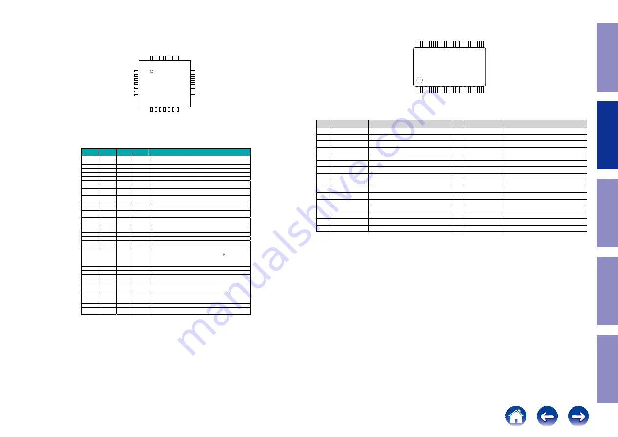
ES9016K2M (AUDIO : U2002)
R
E
S
ET
B
DA
TA
_CLK
DA
TA
1
DA
TA
2
G
P
IO
1
N.
C.
N.
C.
28 27 26 25 24 23 22
DGND
1
21
DVDD
N.C.
2
20
DGND
SCL
3
19
N.C.
SDA
4
18
DVCC
ADDR
5
17
VCCA
XO
6
16
AVCCDAC
XI (MCLK)
7
15
N.C.
8 9 10 11 12 13 14
N.
C.
DA
C
R
DA
C
RB N.
C.
A
G
ND
DA
C
L
D
A
CLB
ES9016K2M
28-QFN
PIN DESCRIPTIONS
Pin
Name
Pin Type
Reset
State
Pin Description
1
DGND
Ground
Ground Digital Ground
2
N.C.
-
-
No internal connection. Pin may be grounded if desired.
3
SCL
I
Tri-stated I
2
C Serial Clock Input
4
SDA
I/O
Tri-stated I
2
C Serial Data Input/Output
5
ADDR
I
Tri-stated I
2
C Address Select
6
XO
AO
Floating XTAL Out
7
XI (MCLK)
AI
Floating XTAL / MCLK In
8
N.C.
-
-
No internal connection. Pin may be grounded if desired.
9
DACR
AO
Driven to
ground
Differential Positive Analog Output Right
10
DACRB
AO
Driven to
ground
Differential Negative Analog Output Right
11
N.C.
-
-
No internal connection. Pin may be grounded if desired.
12
AGND
Ground
Ground Analog Ground
13
DACL
AO
Driven to
ground
Differential Positive Analog Output Left
14
DACLB
AO
Driven to
ground
Differential Negative Analog Output Left
15
N.C.
-
-
No internal connection. Pin may be grounded if desired.
16
AVCCDAC
Power
Power
Analog AVCC for DAC
17
VCCA
Power
Power
1.8V or +3.3V for OSC
18
DVCC
Power
Power
D1.8V to +3.3V
19
N.C.
-
-
No internal connection. Pin may be grounded if desired.
20
DGND
Ground
Ground Digital Ground
21
DVDD
Power
Power
Digital Core Voltage, nom1.2V, is supplied by a regulator from
VCCA. DVDD must be decoupled with a minimum 4.7 F capacitor to
DGND for stable operation. DVDD needs to be externally supplied for
high XI / MCLK frequency. Please refer to the section about the DVDD
supply on page 8 for additional information.
22
N.C.
-
-
No internal connection. Pin may be grounded if desired.
23
N.C.
-
-
No internal connection. Pin may be grounded if desired.
24
GPIO1
I/O
Tri-stated GPIO 1
25
DATA2
I
Tri-stated DSD Data2 (R) or PCM Data CH1/CH2 or SPDIF Input 2
26
DATA1
I/O
Tri-stated
Master mode off: Input for DSD Data1 (L) or PCM Frame Clock or SPDIF
Input 3
Master mode on: Output for PCM Frame Clock
27
DATA_CLK
I/O
Tri-stated
Master mode off: Input for PCM Bit Clock or DSD Bit Clock or SPDIF
Input 1
Master mode on: Output for PCM Bit Clock
28
RESETB
I
Tri-stated Master Reset / Power Down (active low)
Exposed
Pad
DGND
Ground
Ground Digital Ground. Connect the Exposed Pad to DGND
Notes:
-
There are 7 N.C. (No Connect) pins. If desired, these pins can be connected to ground on the PCB to strengthen the
otherwise isolated pin pads.
-
The exposed pad must be connected to digital ground.
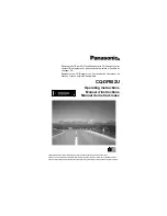
NJU72343_J (AUDIO : U2007)
No. Symbol
Function
No. Symbol
Function
1
AREF
Analog reference potential
17 DATA
IC control data input
2
ADR
Address selection
18 CLOCK
IC control clock input
3
InA2
Ach input2
19 VDDOUT
Digital power supply output
4
InB2
Bch input2
20 AREF
Analog reference potential
5
InA1
Ach input1
21 OutH
Hch output
6
InB1
Bch input1
22 OutG
Gch output
7
InC
Cch input
23 OutF
Fch output
8
InD
Dch input
24 OutE
Ech output
9
InE
Ech input
25 OutD
Dch output
10 InF
Fch input
26 OutC
Cch output
11 InG1
Gch input1
27 OutB
Bch output
12 InH1
Hch input1
28 OutA
Ach output
13 InG2
Cch input2
29 AREF
Analog reference potential
14 InH2
Dch input2
30 V-
Power supply(-)
15 MUTE
External mute control
31 AREF
Analog reference potential
16 REF
Digital reference potential
32 V+
Power )
1
16
17
32
Before Servicing
This Unit
Electrical
Mechanical
Repair Information
Updating
31


