background image

3

dc2326af

DEMO MANUAL DC2326A

Dc2326a setup

+

+

IN0

IN0

+

IN0

V

CM

R107

U25B

LT6237IDD

U25A

LT6237IDD

C96

0.1µF

C94

1000pF

C98

OPT

C116

OPT

R129

1k

R108

49.9Ω

R123

49.9Ω

C104

0.1µF

V

CC

V

EE

R124

C100

OPT

C112

OPT

EN

C102

1000pF

dc2326 F02

R113

R119

1k

DC Power 

The DC2326A requires ±9VDC and draws +145mA/–65mA. 

Most of the supply current is consumed by the FPGA, 

opamps, regulators and discrete logic on the board. The 

±9VDC input voltage powers the ADC through LT1763 

regulators  which  provide  protection  against  accidental 

reverse bias. Additional regulators provide power for the 

FPGA and opamps. 

Clock Source

You must provide a low jitter 2.5V

P-P

 sine or square wave 

to the clock input, J1. The clock input is AC coupled so the 

DC level of the clock signal is not important. A generator 

such as the Rohde & Schwarz SMB100A high speed clock 

source is recommended to drive the clock input. Even a 

good generator can start to produce noticeable jitter at 

low frequencies. Therefore it is recommended for lower 

sample rates to divide down a higher frequency clock to 

the desired sample rate. The ratio of clock frequency to 

conversion rate is shown in the Assembly Options table. If 

the clock input is to be driven with logic, it is recommended 

that  the 49.9Ω termination  resistor (R4)  be  removed. 

Driving R4 with discrete logic may result in slow rising 

edges. These slow rising edges may compromise the SNR 

of the converter in the presence of high-amplitude higher 

frequency input signals. 

Data Output

Parallel data output from this board (0V to 2.5V default), 

if not connected to the DC890, can be acquired by a logic 

analyzer, and subsequently imported into a spreadsheet, or 

mathematical package depending on what form of digital 

signal processing is desired. Alternatively, the data can 

be fed directly into an application circuit. Use pin 50 of 

P1 to latch the data. The data should be latched using the 

negative edge of this signal. The data output signal levels 

at P1 can also be increased to 0V-3.3V if the application 

circuit requires a higher voltage. This is accomplished by 

moving JP2 to the 3.3V position.

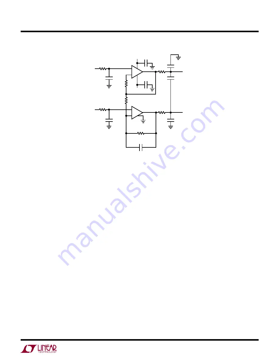
Figure 2. 0V–4.096V Single-Ended to Fully Differential DC Coupled Driver

Содержание LTC2345

Страница 1: ...l and SoftSpan are trademarks of Linear Technology Corporation All other trademarks are the property of their respective owners assembly options Board Photo demonstrate DC performance such as peak to peak noise and DC linearity Use the DC890 if precise sampling rates are required or to demonstrate AC performance such as SNR THD SINAD and SFDR The DC2326A is intended to demonstrate recommended grou...

Страница 2: ...lp menu Updates can be downloaded from the Tools menu Check for updates periodically as new features may be added The PScope software should recognize the DC2326A and configure itself automatically Click the Collect button See Figure 3 to begin acquiring data The Collect button then changes to Pause which can be clicked to stop data acquisition dc590 dc2026 Quick Start Procedure IMPORTANT To avoid...

Страница 3: ...it is recommended for lower sample rates to divide down a higher frequency clock to the desired sample rate The ratio of clock frequency to conversion rate is shown in the Assembly Options table If theclockinputistobedrivenwithlogic itisrecommended that the 49 9Ω termination resistor R4 be removed Driving R4 with discrete logic may result in slow rising edges TheseslowrisingedgesmaycompromisetheSN...

Страница 4: ...Options button in the PScope tool bar shown in Figure 4 This will open the Configure Channels menu of Figure 5 In this menu it is possible to set the input signal range setting for each channel There is also a button to return PScope to the default DC2326A settings which are optimized for the default hardware settings of the DC2326A Thereareanumberofscenariosthatcanproducemislead ing results when ...

Страница 5: ...of a symmetricallayoutaroundtheanaloginputswillminimize theeffectsofparasiticelements Shieldanaloginputtraces with ground to minimize coupling from other traces Keep traces as short as possible Component Selection When driving a low noise low distortion ADC such as the LTC2345 component selection is important so as to not degrade performance Resistors should have low values to minimize noise and d...

Страница 6: ...6 dc2326af DEMO MANUAL DC2326A DC2326A Setup Figure 3 PScope Screen Shot Figure 4 PScope Tool Bar ...

Страница 7: ...7 dc2326af DEMO MANUAL DC2326A DC2326A Setup Figure 5 PScope Configuration Menu ...

Страница 8: ...8 dc2326af DEMO MANUAL DC2326A DC2326A Setup Figure 6 QuikEval Screen Shot Figure 7 QuikEval Configuration Menu ...

Страница 9: ... logic levels The default setting is CMOS Only CMOS is currently supported Definitions P1 DC890 interface is used to communicate with the DC890 controller J1 CLK provides the master clock for the DC2326A when interfaced to the DC890 J2 FPGA PROGRAM is used to program the FPGA This is for factory use only JP4 EEPROM is for factory use only The default posi tion is WP JP5 JP12 AIN0 AIN7 can be used ...

Страница 10: ...UDING ANY WARRANTY OF MERCHANTABILITY OR FITNESS FOR ANY PARTICULAR PURPOSE EXCEPT TO THE EXTENT OF THIS INDEMNITY NEITHER PARTY SHALL BE LIABLE TO THE OTHER FOR ANY INDIRECT SPECIAL INCIDENTAL OR CONSEQUENTIAL DAMAGES The user assumes all responsibility and liability for proper and safe handling of the goods Further the user releases LTC from all claims arising from the handling or use of the goo...

Отзывы: