


3. TECHNICAL BRIEF
- 66 -
3.23. RF synthesizer
The transceiver contains a fractional-N sigma-delta synthesizer for the frequency synthesis in the RX
operation mode. For TX operation mode the fractional-N sigma-delta synthesizer is used as Sigma-
Delta modulation loop to process the phase/frequency signal. The 26MHz reference signal is provided
by the internal crystal oscillator. This frequency serves as comparison frequency of the phase detector
and as clock frequency for all digital circuitry.The divider in the feedback path of the synthesizer is
carried out as a multi-modulus divider (MMD). The loop filter is fully integrated and the loop bandwidth
is about 100 kHz to allow the transfer of the phase modulation. The loop bandwidth is automatically
adjusted prior to each slot (OLGA©˜). To overcome the statistical spread of the loop filter element
values an automatic loop filter adjustment (ALFA) is performed before each synthesizer startup. The
fully integrated quad-band VCO is designed for the four GSM bands (850, 900, 1800, 1900 MHz) and
operates at double or four times transmit or receive frequency. To cover the wide frequency range the
VCO is automatically aligned by a binary automatic band selection (BABS) before each synthesizer
startup.
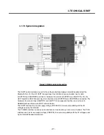
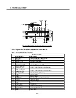
3.24. VCTCXO
The VCTCXO (X401) supply 26MHz reference clock and controlled by AFC input to generate a strict
system clock. The 26MHz clock is used to Transceiver(U402), Bluetooth chip(U102) and S-Gold2
(U102).
Figure 40 VCTCXO Schematic
C430
22p
X401
GND
2
3
OUT
VCC
4
VCONT
1
26MHz
R425
620
2V7_VCXO
C431
1uF
NA
C455
0
R449
AFC
Содержание KE820
Страница 1: ...Service Manual Model KE820 Service Manual KE820 Date August 2006 Issue 1 0 ...
Страница 3: ... 4 ...
Страница 5: ... 6 ...
Страница 46: ...3 TECHNICAL BRIEF 47 Figure 18 EN SET port control method ...
Страница 69: ...4 PCB layout 70 Figure 45 Main PCB bottom Figure 46 Main PCB bottom placement ...
Страница 70: ...4 PCB layout 71 Figure 47 Sub PCB top Figure 48 Sub PCB top placement ...
Страница 71: ...4 PCB layout 72 Figure 49 Sub PCB bottom Figure 50 Sub PCB bottom placement ...
Страница 114: ...6 Download S W upgrade 115 6 2 Download program user guide ...
Страница 115: ... 116 6 Download S W upgrade ...
Страница 116: ... 117 6 Download S W upgrade ...
Страница 117: ... 118 6 Download S W upgrade ...
Страница 124: ... 125 8 PCB LAYOUT ...
Страница 125: ... 126 8 PCB LAYOUT ...
Страница 126: ... 127 8 PCB LAYOUT ...
Страница 127: ... 128 8 PCB LAYOUT ...
Страница 129: ...9 RF Calibration 130 9 2 3 Click SETTING Menu 9 2 4 Setup Ezlooks menu such as the following figure ...
Страница 131: ...9 RF Calibration 132 9 2 7 Select MODEL 9 2 8 Click START for RF calibration 9 2 9 RF Calibration finishes ...
Страница 132: ...9 RF Calibration 133 9 2 10 Calibration data will be saved to the following folder Saving format year month day_PASS ...
Страница 136: ... 137 11 STANDALONE TEST 4 Click Update Info for communicating Phone and Test Program Connected ...
Страница 141: ... 142 ...
Страница 161: ...Note ...
Страница 162: ...Note ...


