


3. TECHNICAL BRIEF
- 42 -
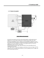
3.7. LCD Display
LCD module include:
- LCD : 220 x 176 265K Colors TFT LCD
- Backlight : 4 piece of white LED illumination
LCD module is connected to main board thru 30 pins connector.
LCD FPC Interface Spec:
Table 7 LCD FPC Interface Spec.
Pin No. Pin Name
I/O
Description
1 GND
-
Ground
2
2V8_VDD
Power
LCD power supply
3
2V8_Vci
Power
LCD power supply
4 LCD_RESET I
LCD
reset
5 GND
I/O Ground
6
L_D(0)
I/O
Data[0] for LCD
7
L_D(1)
I/O
Data[1] for LCD
8
L_D(2)
I/O
Data[2] for LCD
9
L_D(3)
I/O
Data[3] for LCD
10
L_D(4)
I/O
Data[4] for LCD
11
L_D(5)
I/O
Data[5] for LCD
12
L_D(6)
I/O
Data[6] for LCD
13
L_D(7)
I/O
Data[7] for LCD
14 GND
-
Ground
15 GND
-
Ground
16 GND
-
Ground
17
MLED_A
I
BLU LED common Anode
18
MLED_C1
O
BLU LED1 Cathode
19
MLED_C2
O
BLU LED2 Cathode
20
MLED_C3
O
BLU LED3 Cathode
21
MLED_C4
O
BLU LED4 Cathode
22 GND
-
Ground
23
L_CS
I
LCD chip select
24 L_RD(N.C.)
I
Read
strobe
25
L_ADS
I
Address data switch
26 L_WR
I
Write
strobe
27 GND
-
Ground
28 Vsync(N.C.) O
Vertical
sync
29
LCD_ID
O
LCD maker Identification
30 GND
-
Ground
Содержание KE820
Страница 1: ...Service Manual Model KE820 Service Manual KE820 Date August 2006 Issue 1 0 ...
Страница 3: ... 4 ...
Страница 5: ... 6 ...
Страница 46: ...3 TECHNICAL BRIEF 47 Figure 18 EN SET port control method ...
Страница 69: ...4 PCB layout 70 Figure 45 Main PCB bottom Figure 46 Main PCB bottom placement ...
Страница 70: ...4 PCB layout 71 Figure 47 Sub PCB top Figure 48 Sub PCB top placement ...
Страница 71: ...4 PCB layout 72 Figure 49 Sub PCB bottom Figure 50 Sub PCB bottom placement ...
Страница 114: ...6 Download S W upgrade 115 6 2 Download program user guide ...
Страница 115: ... 116 6 Download S W upgrade ...
Страница 116: ... 117 6 Download S W upgrade ...
Страница 117: ... 118 6 Download S W upgrade ...
Страница 124: ... 125 8 PCB LAYOUT ...
Страница 125: ... 126 8 PCB LAYOUT ...
Страница 126: ... 127 8 PCB LAYOUT ...
Страница 127: ... 128 8 PCB LAYOUT ...
Страница 129: ...9 RF Calibration 130 9 2 3 Click SETTING Menu 9 2 4 Setup Ezlooks menu such as the following figure ...
Страница 131: ...9 RF Calibration 132 9 2 7 Select MODEL 9 2 8 Click START for RF calibration 9 2 9 RF Calibration finishes ...
Страница 132: ...9 RF Calibration 133 9 2 10 Calibration data will be saved to the following folder Saving format year month day_PASS ...
Страница 136: ... 137 11 STANDALONE TEST 4 Click Update Info for communicating Phone and Test Program Connected ...
Страница 141: ... 142 ...
Страница 161: ...Note ...
Страница 162: ...Note ...


