- 72 -
LGE Internal Use Only
Copyright © 2009 LG Electronics. Inc. All right reserved.
Only for training and service purposes
3. Technical brief
C. Synthesizer
The RX and TX RF VCOs are fully integrated and self-calibrated on manufacturing tolerances.
They have 16 different frequency ranges that are selected internally depending on the frequency
programming. The calibration is done on each low to high logical transition of the SYNON bit in the
control register or on each change of the integer divider ratio of the RF fractional N synthesizer.
A high-performance RF fractional-N synthesizer PLL is included on-chip which enables the
frequency of the RF VCO to be synthesized. The frequency is set through the 3-wire serial
programming bus. The PLL is based on Sigma-Delta (
Σ
.) fractional-N synthesis that enables the
required channel frequency, including Automatic Frequency Control (AFC) from a free running
external 26 MHz reference frequency. Very low close-in-phase noise is achieved. This allows
widening of the PLL loop bandwidth and shorter settling time. The programmable main dividers
are controlled by a second order
Σ
-modulus controller. They divide the RF VCO signals down to
frequencies of 26 MHz (12 Hz step programmability). Their phase is then compared in a digital
Phase/Frequency Detector (PFD) to the 26 MHz reference clock signal.
The phase error information is fed back to the RF VCO through the charge pump circuit
that .sources. into or .sinks. current from the loop filter capacitor, thus changing the VCO
frequency such that the loop finally gets phase-locked.
1
0
1
C
p
6
5
2
0
1
C
I
N
D
0603
7
0
1
C
p
2
2
p
2
2
8
0
1
C
3
0
6
0
5.
6n
L1
0
4
p
2
2
1
1
1
C
0603
0
2
2
2
0
1
R
3
0
6
0
3
0
6
0
0
2
2
3
0
1
R
I
N
D
7
3
1
C
8
V
2
_
A
D
A
R
V
p
6
5
8
1
1
C
2.
4n
L
105
8
V
2
_
A
D
A
R
V
0603
8
2
1
C
p
0
1
3
0
6
0
p
0
1
6
2
1
C
0
2
2
6
0
1
R
3
0
6
0
0
2
2
7
0
1
R
3
0
6
0
8
V
2
_
A
D
A
R
V
8
V
2
_
A
D
A
R
V
p
2
.
8
8
3
1
C
I
N
D
9
3
1
C
8
V
1
_
D
A
R
G
I
D
V
0
0
F
0
A
F
4
1
G
2
B
E
F
A
S
2
0
1
L
F
4
5
1
3
2
G1
O1
IN
G2
O2
0
0
F
0
A
K
5
9
G
1
B
E
F
A
S
3
0
1
L
F
2
5
1
4
3
3
G
N
I
T
U
O
1
G
2
G
6
0
1
U
N
H
5
9
1
6
M
O
_
0
0
1
3
F
R
20
19
18
17
16
15
14
13
12
11
1
2
0
1
2
2
9
3
2
8
4
2
7
5
2
6
6
2
5
7
2
4
8
2
3
9
2
2
0
3
1
31
32
33
34
35
36
37
38
39
40
41
PG
N
D
VC
C
T
X
RF
_DAC2
RF
_DAC1
NC13
MI
X
1
_
B
MI
X
1
_
A
NC12
NC11
NC10
VC
C
R
X
X
T
D
N
G
9
C
N
1
C
N
T
U
O
_
1
A
N
L
2
C
N
8
C
N
1
_
X
T
N
I
_
1
A
N
L
3
C
N
7
C
N
X
T
O
L
C
C
V
6
C
N
A
I
X
T
X
R
O
L
C
C
V
B
I
X
T
5
C
N
A
Q
X
T
D
D
V
B
Q
X
T
T
S
T
VG
A
C
T
L
DAT
A
CL
K
EN
RE
F
IN
NC4
RX
IA
RX
IB
RX
Q
A
RX
Q
B
7
5
1
C
p
6
5
1
_
D
N
A
B
_
X
R
W
P
_
I
_
X
R
W
N
_
I
_
X
R
W
P
_
Q
_
X
R
W
N
_
Q
_
X
R
W
1
_
D
N
A
B
_
D
O
M
X
T
W
N
_
Q
_
X
T
W
P
_
Q
_
X
T
W
N
_
I
_
X
T
W
P
_
I
_
X
T
W
C
C
V
_
A
P
W
S
A
I
B
_
A
P
W
K
L
C
W
B
R
T
S
_
L
R
T
C
_
F
R
A
T
A
D
_
L
R
T
C
_
F
R
K
L
C
_
L
R
T
C
_
F
R
3
0
6
0
3
0
6
0
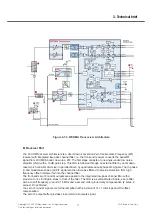
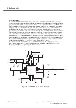
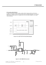
Figure 3-7-4. WCDMA Transceiver schematic
Содержание GD580
Страница 1: ...Service Manual Model GD580 Internal Use Only Service Manual GD580 Date November 2009 Issue 1 0 ...
Страница 179: ... 180 LGE Internal Use Only Copyright 2009 LG Electronics Inc All right reserved Only for training and service purposes ...
Страница 189: ... 190 LGE Internal Use Only Copyright 2009 LG Electronics Inc All right reserved Only for training and service purposes ...
Страница 203: ... 204 LGE Internal Use Only Copyright 2009 LG Electronics Inc All right reserved Only for training and service purposes ...
Страница 211: ... 212 LGE Internal Use Only Copyright 2009 LG Electronics Inc All right reserved Only for training and service purposes ...


