background image

- 89 -

Copyright © 2009 LG Electronics. Inc. All right reserved.
Only for training and service purposes

LGE Internal Use Only

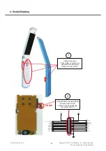
4. Trouble Shooting

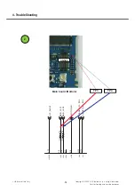
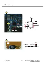
< Main Board – Bottom side >

2

TP 3

TP 4

TP4

TP3

U503

0

1

5

C

U

1

U

1

6

1

5

C

8

V

1

_

M

A

C

_

D

D

V

T

A

B

V

3

0

5

U

1

0

0

9

1

3

0

Y

S

U

E

W

Q

P

G

M

-

1

1

0

9

T

R

9

5

4

6

3

7

2

8

1

N

I

V

1

T

U

O

V

1

N

E

2

T

U

O

V

2

N

E

2

C

N

1

C

N

D

N

G

PG

N

D

8

V

2

_

M

A

C

_

D

D

V

9

1

5

C

U

1

N

E

_

O

D

L

_

M

A

C

_

P

G

_

P

P

A

TP3

TP4

Содержание GD580

Страница 1: ...Service Manual Model GD580 Internal Use Only Service Manual GD580 Date November 2009 Issue 1 0 ...

Страница 2: ...t Trouble 81 4 4 MicroSD card Trouble 82 4 5 Key and Touch Screen Trouble 83 4 6 Camera Trouble 85 4 7 Main LCD Trouble 92 4 8 Keypad Backlight Trouble 96 4 9 Audio Trouble Shooting 99 4 10 Charger Trouble Shooting 113 4 11 Bluetooth Trouble 116 4 12 RF Component 119 4 13 Procedure to check 120 4 14 Checking Common Power Source Block 121 4 15 Checking VCXO Block 128 4 16 Checking Front End Module ...

Страница 3: ... 4 LGE Internal Use Only Copyright 2009 LG Electronics Inc All right reserved Only for training and service purposes ...

Страница 4: ...e of facilities accessed through or connected to it LGE will not be responsible for any charges that result from such unauthorized use B Incidence of Harm If a telephone company determines that the equipment provided to customer is faulty and possibly causing harm or interruption in service to the telephone network it should disconnect telephone service until repair can be done A telephone company...

Страница 5: ...d Attenuation KM555E may interfere with sensitive laboratory equipment medical equipment etc Interference from unsuppressed engines or electric motors may cause problems H Electrostatic Sensitive Devices ATTENTION Boards which contain Electrostatic Sensitive Device ESD are indicated by the sign Following information is ESD handling Service personnel should ground themselves by using a wrist strap ...

Страница 6: ... Signal Processing EEPROM Electrical Erasable Programmable Read Only Memory EGPRS Enhanced General Packet Radio Service EL Electroluminescence ESD Electrostatic Discharge FPCB Flexible Printed Circuit Board GMSK Gaussian Minimum Shift Keying GPIB General Purpose Interface Bus GPRS General Packet Radio Service GSM Global System for Mobile Communications IPUI International Portable User Identity IF ...

Страница 7: ...uare RTC Real Time Clock SAW Surface Acoustic Wave SIM Subscriber Identity Module SLR Sending Loudness Rating SRAM Static Random Access Memory STMR Side Tone Masking Rating TA Travel Adapter TDD Time Division Duplex TDMA Time Division Multiple Access UART Universal Asynchronous Receiver Transmitter VCO Voltage Controlled Oscillator VCTCXO Voltage Control Temperature Compensated Crystal Oscillator ...

Страница 8: ...t 103 5g 87 0g With out Battery Power 800mAh Li Ion Talk Time Over 170 Min WCDMA Tx 12dBm Voice Over 180 Min GSM Tx Max Voice Stand by Time Over 250 hours WCDMA DRX 7 GSM Paging period 5 Antenna Intenna Type LCD Main 240x400Pixel Back Light Yes Back Light color White Vibrator Yes Coin Type Speaker Yes MIC Yes SMT Type 2EA 1 for speaker phone 1 for Voice call Receiver Yes Earphone Jack Yes SIM Sock...

Страница 9: ...ning and service purposes 2 Performance 2 2 Usable environment 1 Environment 2 Environment Accessory CLA 12 24V DC Item Spec Unit Voltage 3 7 Typ 3 4 Min Shut Down 3 2 V Operating Temp 20 60 C Storage Temp 30 85 C Humidity max 85 Item Spec Min Typ Max Unit Power Available power 100 220 240 Vac ...

Страница 10: ... 47dBm 1G 1 71GHz 47dBm 1G 1 85GHz 47dBm 1 71G 1 785GHz 53dBm 1 71G 1 785GHz 53dBm 1 85G 1 91GHz 53dBm 1 785G 12 75GHz 47dBm 1 785G 12 75GHz 47dBm 1 91G 12 75GHz 47dBm Radiated Spurious Emission MS allocated Channel 30M 1GHz 36dBm 30M 1GHz 36dBm 30M 1GHz 36dBm 1G 1710MHz 30dBm 1G 4GHz 30dBm 1710M 1785MHz 36dBm 1G 4GHz 30dBm 1785M 4GHz 30dBm Idle Mode 30M 880MHz 57dBm 30M 880MHz 57dBm 30M 880MHz 57...

Страница 11: ...ansient 400kHz 19dB 400kHz 22dB 400kHz 22dB 600kHz 21dB 600kHz 24dB 600kHz 24dB 1200kHz 21dB 1200kHz 24dB 1200kHz 24dB 1800kHz 24dB 1800kHz 27dB 1800kHz 27dB 7 Intermodulation attenuation Frequency offset 800kHz Intermodulation product should be Less than 50dB below the level of Wanted signal 8 Transmitter Output Power Power control Power Power control Power Toleran ce Power control Power Toleran ...

Страница 12: ...erence between UE Power setting in uplink compressed 3dB after 14slots transmission gap Inner Loop Power control in uplink Adjust output TPC command cmd 1dB 2dB 3dB 1 0 5 1 5 1 3 1 5 4 5 0 0 5 0 5 0 5 0 5 0 5 0 5 1 0 5 1 5 1 3 1 5 4 5 group 10equal command group 1 8 12 16 24 Occupied Bandwidth OBW 5MHz 99 Out of synchronization handling of output power Qin Qout DPCCH quality levels Toff DPCCH lor ...

Страница 13: ...6dBm f 9 150KHz 1k BW 36dBm f 150KHz 30MHz 10k 36dBm f 30 1000MHz 100k 30dBm f 1 12 75GHz 1M 41dBm 1893 5 1919 6MHz 300k 67dBm 925 935MHz 100k 79dBm 935 960MHz 100k 71dBm 1805 1880MHz 100k Transmit OFF Power 15dB SF 4 768kbps multi code transmission Transmit Intermodulation 31dBc 5MHz Interferer 40dBc 41dBc 10MHz Interferer 40dBc Error Vector Magnitude EVM 17 5 20dBm 12 2k 1DPDCH 1DPCCH ...

Страница 14: ...rer 44dBm 2 Co Channel Rejection TCH FS Class II RBER TUhigh FH C Ic 7dB C Ic 7dB 3 Adjacent Channel Rejection Speech Channel 200kHz C Ia1 12dB C Ia1 12dB C Ia2 44dB C Ia2 44dB 4 Intermodulation Rejection Wanted Signal 98dBm Wanted Signal 96dBm 1 st interferer 44dBm 1 st interferer 44dBm 2 nd interferer 45dBm 5 Blocking Response TCH FS Class II RBER Wanted Signal 101dBm Unwanted Signal Depend on f...

Страница 15: ...er class3 57dBm f 9KHz 1GHz 100k BW 4 In band Blocking 56dBm 3 84MHz 10MHz UE 20dBm output power class3 44dBm 3 84MHz 15MHz UE 20dBm output power class3 5 Out band Blocking 44dBm 3 84MHz f 2050 2095 2185 2230MHz band a UE 20dBm output power class3 30dBm 3 84MHz f 2025 2050 2230 2255MHz band a UE 20dBm output power class3 15dBm 3 84MHz f 1 2025 2255 12500MHz band a UE 20dBm output power class3 Item...

Страница 16: ... 36dBm 57dBm Above 1GHz 12 75GHz 30dBm 47dBm 1 8 1 9GHz 47dBm 47dBm 5 15 5 3GHz 47dBm 47dBm Specification Carrier Frequency Drift Modulation Characteristics Power Control 2dB step size 8dB fmax fmin below the level of 30dBm 100khz BW Class 2 6 4dBm Power density 20dBm per 100kHz EIRP 9 5 Out of Band Spurious Emissions 5 slot 40kHz Maximum drift rate 20KHz 50usec within 2 4GHz 2 4835GHz 1MHz 20dBm ...

Страница 17: ... 3MHz Adjacent 3MHz interference to in band mirror frequency C I image 1MHz interfering Signal Frequency 30MHz 2000MHz 2000MHz 2400MHz 2500MHz 3000MHz 3000MHz 12 75GHz 16 Maximum Input Level C I performance Blocking Characteristic Intermodluation Performance BER 0 1 70dBm BER 0 1 70dBm 11dB 0dB 30dB BER 0 1 20dBm BER 0 1 wanted signal 67dBm 27dBm 27dBm 10dBm BER 0 1 wanted signal 64dBm Power Level...

Страница 18: ... 54 0 05V BAR 1 4 Icon Blinking Alerting Sound 3 43 0 05V POWER OFF 3 20 0 05V Stand by Voice Call VT WCDMA 250 Hours 3 2 mA DRX 7 170 Min 270 mA Tx 12dBm 100 Min 450mA Tx 12dBm GSM 250 Hours 3 2 mA Paging period 5 180 Min 260 mA Tx Max GSM WCDMA BAR 7 5 93 2dBm 90 2dBm BAR 5 4 98 2dBm 103 2dBm BAR 4 2 101 2dBm 107 2dBm BAR 2 1 104 2dBm 109 2dBm BAR 1 0 106 2dBm 111 2dBm VT test Speaker off LCD ba...

Страница 19: ... Sending INS Refer to TABLE 30 3 7 4 Echo Loss EL 54dBm0p below NOM MAX NOM MAX NOM MAX NOM MAX 9 10 11 Receiving Loudness Rating RLR 12 Echo Loss EL Sending Loudness Rating SLR Side Tone Masking Rating STMR 12 3dB 1 3dB 25dB over HEAD SET 8 3dB 40dB over 13 14 NOM MAX NOM MAX SEND REV Sending Distortion SD Refer to TABLE 30 3 15 Idle Noise Sending INS 55dBm0p below Receiving Distortion RD Refer t...

Страница 20: ...Voltage 4 2V Charging Current 500mA below Await mode In case of During a Call should be kept 3 9V GSM It should be kept 3 9V in all power level WCDMA It will not be kept 3 9V in some power level Extend await mode At Charging prohibited temperature 0 C under or 45 C over GSM It should be kept 3 7V in all power level WCDMA It will not be kept 3 7V in some power level ...

Страница 21: ... together with a tightly coupled memory The DSP is the Ceva X 1620 core with a 64 kB instruction RAM and a 64 kB data RAM It also contains debug logic and interfaces In addition to the mega cell the DSPSUB includes external memories peripheral units and interfaces The DSP mega cell is clocked at 208 MHz The DSPSUB includes an AHB master and an AHB slave interface The AHB master provides a direct a...

Страница 22: ... 23 Copyright 2009 LG Electronics Inc All right reserved Only for training and service purposes LGE Internal Use Only 3 Technical brief Figure 3 1 1 GD580 Block Diagram GD580 Block Diagram ...

Страница 23: ...ation data etc are stored in flash memory area A GD580 y 2Gb NAND flash memory 1Gb SDRAM Table 3 1 1 External Memory Interface Spec of GD580 Figure 3 1 2 External Memory Configuration of GD580 Device Part Name Maker Item Time Size Speed Program speed 220μs 1 page 2K 64 Byte 2 64MByte s Erase speed 1 5ms 1 Block 128K 4K Byte 8MByte s NAND flash KA100J00BA AJYY Samsung y Package 107 ball FBGA Type 1...

Страница 24: ...t 2009 LG Electronics Inc All right reserved Only for training and service purposes LGE Internal Use Only 3 Technical brief 3 1 3 Hardware Architecture A Block Diagram Figure 3 1 3 Access system of Ericsson DB3150 ...

Страница 25: ... 26 LGE Internal Use Only Copyright 2009 LG Electronics Inc All right reserved Only for training and service purposes 3 Technical brief Figure 3 1 4 Application system of Ericsson DB3150 ...

Страница 26: ... which provide a simple interface to support different timing and memory access arrangements D DSP Hardware Subsystem The Digital Signal Processor Subsystem DSPSUB includes a DSP mega cell which contains the DSP CPU together with a tightly coupled memory The DSP is the Ceva X 1620 core with a 64 kB instruction RAM and a 64 kB data RAM It also contains debug logic and interfaces In addition to the ...

Страница 27: ...A GSM Radio Link Interface DB3150 controls GSM RF part using these signals through GSM RF chip RF3000 y RF_DATA_A y RF_DATA_B y RF_DATA_C y RF_DATA_STRB Figure 3 1 5 Schematic of GSM RF Interface B WCDMA Radio Link Interface y RF_WCDMA_PA_0_EN y RF_WCDMA_PA_1_EN y RF_WCDMA_DCDC_EN y RF_WCDMA_PWRDET_EN Figure 3 1 6 Schematic of WCDMA RF Interface Y2 Y3 AA2 Y4 RF_DATA_A RF_DATA_B RF_DATA_C RF_DATA_S...

Страница 28: ...een DBB and ABB SIMDAT0 SIM card bidirectional data line SIMCLK0 SIM card reference clock SIMRST0 SIM card async sync reset VDD DAT CLK CARD RST SIMVCC AB3000 SDAT SIMDAT SCLK SIMCLK SRST SIMRST DB3150 SIMDAT0 SIMCLK0 SIMRST0 VDD E 10K 10K 3 1 6 UART Interface UART signals are connected to DB3150 GPIO through IO connector Table 3 1 3 UART Interface UART0 Resource Name Note ACC_GPIO_2 ACC_GP02_UART...

Страница 29: ...ACC_USB_RCV Input ACC_GPIO_5 ACC_USB_VBDET Input ACC_GPIO_6 ACC_GP_LED_M_RES_M Output low ACC_GPIO_7 ACC_GP_LED_M_LDO_EN Output low ACC_GPIO_8 NA Output low ACC_GPIO_9 ACC_GP_HF_MIC_BIAS_EN Output low ACC_GPIO_10 NA Output Low ACC_GPIO_11 NA Output Low ACC_GPIO_12 ACC_GP_BT_SPI_INT Input ACC_GPIO_13 ACC_GP_FLIPSENSE Input ACC_GPIO_14 ACC_GP_FM_RDY Output low ACC_GPIO_15 ACC_GP_PHFSENSE Input ACC_G...

Страница 30: ...ART_TX Output low APP_GPIO_2 APP_GP_3MCAM_SDN Output high APP_GPIO_3 APP_GP_CAM_LDO_EN Output low APP_GPIO_4 APP_GP_FM_SDA Output low APP_GPIO_5 APP_GP_LED_M_BOOST_EN Output low APP_GPIO_6 APP_GP_MMC_DET Input APP_GPIO_7 APP_GP_3AXIS_INT Input APP_GPIO_8 APP_GP_3AXIS_SDA Input APP_GPIO_9 APP_GP_3AXIS_SCL Output high APP_GPIO_10 APP_GP_LCD_BL_CTRL Output high APP_GPIO_11 APP_GP_MMC_CLKRET Output lo...

Страница 31: ...iate external ULPI transceiver with the built in multiplexer y Full speed PHY using a standard 4 pin differential interface with DP DM OE and RCV and sideband signaling for USBVbus detect PullUpEnable and suspend This mode only supports USB full speed device operation USB UART multiplexing is possible by selecting the appropriate external full speed transceiver with the built in multiplexer y Full...

Страница 32: ... U _ C C A N E U P _ B S U _ C C A D N P S U S _ B S U _ C C A K 0 0 1 2 2 3 R 6 1 _ O I P G _ C C A N O C D M4 L3 L4 USB_DAT_VP USB_SE0_VM USB_OE USB_DAT_VM USB_OE USB_DAT_VP U 2 2 3 0 6 C 7 0 6 C U 1 0 S B 2 0 1 1 P S I 3 0 6 U 7 6 5 4 8 3 9 2 0 1 1 11 12 13 14 15 PGND SOFTCON VPU_3_3 VCC_5_0 VREG_3_3 E O _ C N V C R D O P V _ P V D VM_VMO SUSPND VCC_IO VBUSDET 1 1 6 C U 1 3 3 5 1 6 R 3 3 8 1 6 ...

Страница 33: ...ct the Folder module status Open or Close If a magnet is close to the hall effect switch U100 the voltage at Pin 4 of U100 goes to 0V Otherwise 1 8V This ACC_GP_FILPSENSE signal is delivered to DB3150 ACC_GPIO13 Figure 3 1 10 Folder Open Close Detector 0 0 1 U X V N 1 3 0 2 5 U B 5 2 3 1 4 T U O D D V D N G C N PGND n 0 0 1 2 0 1 C n 0 0 1 1 0 1 C 8 V 1 _ E D D V E S N E S P I L F _ P G _ C C A ...

Страница 34: ...tocol Also synchronous data packet transfer sSCO over HCI is supported The SPI data length and endianness are configurable The SPI interface can only operate in half duplex mode C PCM Interface The PCM interface is used to send audio to and from the Bluetooth module The interface is a synchronous interface using a PCM clock and a PCM sync signal for synchronization Two data signals are used for da...

Страница 35: ...nning D Master Clock and Clock Request Interface The master clock MCLK is a 26 MHz signal used as the high precision clock signal for the Bluetooth module The signal can be switched on and off by the platform The master clock request CLKREQ is used by the Bluetooth module to ask for the master clock If the Bluetooth module asserts the signal high it gets the master clock The other alternative for ...

Страница 36: ...5 2 DH1 2 DH3 2 DH5 3 DH1 3 DH3 3 DH5 SCO HV1 HV3 and DV eSCO EV3 EV4 EV5 2 EV3 2 EV5 3 EV3 3 EV5 Adaptive Frequency Hopping AFH Channel Quality Driven Data Rate CQDDR Lisbon Feature Encryption Pause Resume EPR Entended Inquiry Response EIR Link Supervision Time Out LSTO Secure Simple Pairing Sniff Subrating Quality of Service QoS Packet Boundary Flag Erroneous Data Delivery Transmit Power Power C...

Страница 37: ...etooth device Communication interfaces Fast UART up to 4 MHz Flexible SPI interface up to 13 MHz PCM interface Up to 10 additional flexibly programmable GPIOs External interrupts possible through the GPIOs Fast I2C interface as master Clock support System clock input digital or sine wave at 9 6 10 13 16 16 8 19 2 26 33 6 or 38 4MHz Low Power clock input at 3 2 32 and 32 768 kHz ARM7TDMI CPU Memory...

Страница 38: ...G _ T B 2 G I D S S V _ T B 0 1 _ O I P G _ T B 3 G I D S S V _ T B 6 1 _ O I P G _ T B 4 G I D S S V _ T B 8 _ O I P G _ T B 5 G I D S S V _ T B 1 A N A S S V _ T B 0 _ O I P G _ T B 2 A N A S S V _ T B 1 _ N I _ Q E R _ K L C _ T B 3 A N A S S V _ T B 2 _ N I _ Q E R _ K L C _ T B 4 A N A S S V _ T B P U E K A W _ T S O H _ T B 5 A N A S S V _ T B 6 A N A S S V _ T B 1 _ G I F N O C _ T B 7 A N ...

Страница 39: ...4 A 4 C 4 B 1 D 2 A 1 C 2 D 2 B 5 C 5 D 5 A A C C V B C C V R I D _ 0 T A D A 0 T A D B 0 T A D R I D _ 3 2 1 T A D A 1 T A D B 1 T A D A 2 T A D B 2 T A D A 3 T A D B 3 T A D R I D _ D M C A D M C A K L C F _ K L C 1 D N G B D M C 2 D N G B K L C U 7 4 4 1 6 C R609 100K R610 100K R611 100K U 1 0 2 1 6 C 3 1 6 C U 1 0 8 V 1 _ E D D V 1 T A D _ D S O R C I M R I D _ T A D _ D S O R C I M R I D _ D ...

Страница 40: ...y and then ONSWAn signal is changed to Low d AB3000 initiates the internal oscillator and powers on the regulators e AB3000 generates power for DB3150 f AB3000 releases the power reset signal PWRRSTn and generates an interrupt IRQ0n to DB3150 Figure 3 1 13 Power On Sequence DB3150 RESPOW_N IRQ0_N AB3000 PWRRST IRQ ONSWA e Power for DB3150 f PWRRSTn f IRQ0n c ONSWAn c Press END key ...

Страница 41: ... U B _ D A P Y E K 1 0 1 B K N O T T U B _ D A P Y E K 0 0 1 B K N O T T U B _ D A P Y E K 6 0 1 B K N O T T U B _ D A P Y E K 7 0 1 B K N O T T U B _ D A P Y E K 5 0 1 B K N O T T U B _ D A P Y E K 4 0 1 B K N O T T U B _ D A P Y E K 3 2 1 B K N O T T U B _ D A P Y E K 0 1 1 B K N O T T U B _ D A P Y E K 9 0 1 B K N O T T U B _ D A P Y E K 8 0 1 B K N O T T U B _ D A P Y E K 1 1 1 B K N O T T U B...

Страница 42: ... set the current value and firefly setting for each forty nine LED drivers Features LED matrix driver 7X7 Step up charge pump DC DC converter 300mA LDO 2 ch GPIO 3 ch I2C Interface LED drivers for RGB 3 ch matrix LED driver 7x7 ch Figure 3 1 15 Matrix LED and RGB LED 9 2 8 1 0 0 1 2 0 3 9 2 6 4 0 1 0 1 N C 1 2 0 2 9 1 8 1 7 1 6 1 5 1 4 1 3 1 2 1 1 1 0 1 9 8 7 6 5 4 3 2 1 T A B V T S O O B V 8 V 1 ...

Страница 43: ...rator Module GAM subsystem provides hardware support in the creation of visual imagery and the transfer of this data to the display GAM also provides support for the camera module The visual data could be graphics still images or video The GAM subsystem consists of five modules y GRAM graphics memory 160 kB y GAMCON GAM controller y GRAPHCON graphics controller y PDI SSI programmable display inter...

Страница 44: ... required to transfer a VGA 640 by 480 pixels image from the camera data interface CDI over DMA at 100 MBit s within a 50 ms timeframe The GRAM is used as a buffer but the average transfer bandwidth required is approximately 3 Mword s 32 bit word that is 12 MByte s C Graphics Controller GRAPHCON Block GRAPHCON is controlled by the application CPU and can perform operations on pixels and image area...

Страница 45: ...ormat on the data bus is YUV 4 2 2 raw binary image data according to the CCIR 656 standard A function within the CDI can be programmed to reorder the YUV parameters as they pass through the CDI In addition the CDI is able to detect the end of an image and perform some truncation as well as overflow conditions There is nothing preventing the use of other data types such as JPEG or RGB as long as t...

Страница 46: ... CI_D7 TP307 P T CI_PCLK LCD_VSYNC LCD_RESN LCD_CSN LCD_ADS LCD_WEN CI_HSYNC CI_VSYNC CI_D7 CI_D6 CI_D5 CI_D4 CI_D3 CI_D2 CI_D1 PDI_D5 PDI_D3 PDI_D1 PDI_D0 LCD_RDN CI_RESN CI_D0 PDI_D7 PDI_D6 PDI_D4 PDI_D2 Figure 3 2 2 Camera Interface in DB3150 1 0 5 N C 0 0 0 3 E 0 1 H S 4 2 2 4 0 B G 1 0 2 4 3 0 0 Y B N E 2 1 3 1 1 1 4 1 0 1 5 1 9 6 1 8 7 1 7 8 1 6 9 1 5 0 2 4 1 2 3 2 2 2 3 2 1 4 2 8 0 5 C U 1 ...

Страница 47: ...U 1 0 0 0 0 1 9 0 5 B F 1 0 7 1 1 0 0 Y E F S R F 0 0 1 R 0 7 0 E 4 8 1 0 1 E V C I 4 0 5 L F 10 5 6 4 7 3 8 2 9 1 1 A _ T U O N I 1 B _ T U O N I 2 A _ T U O N I 2 B _ T U O N I 3 A _ T U O N I 3 B _ T U O N I 4 A _ T U O N I 4 B _ T U O N I G1 G2 8 V 2 _ D C L _ D D V 100K R507 0 0 8 1 1 N S 2 8 1 D H 5 1 M L B 3 0 5 B F 0 0 8 1 1 N S 2 8 1 D H 5 1 M L B 5 0 5 B F 1 5 4 0 5 R A D S _ C 2 I _ P P...

Страница 48: ...Z pixel clo ck 15fps for VGA camera vertical sync signal horizontal sync signal reset signal and 8bits YUV data from camera module The camera module is controlled by I2C port Pin no Symbol Pin no Symbol 1 GND 13 GND 2 CI_D7 14 VDD_CAM_1V8 3 CI_D6 15 VDD_CAM_1V8 4 CI_D5 16 VDD_CAM_2V8 5 CI_D4 17 GND 6 CI_D3 18 SYSCLK0 7 CI_D2 19 CI_HSYNC 8 CI_D1 20 CI_VSYNC 9 CI_D0 21 GND 10 CI_PCLK 22 APP_I2C_SDA ...

Страница 49: ...M_LDO_EN enables 1 8V 2 8V Camera Regulator for both 3M and VGA Camera 3M 2 8V for analog 1 8V for I O 1 8V for digital VGA 2 8V for analog 1 8V for I O digital 0 1 5 C U 1 U 1 6 1 5 C 8 V 1 _ M A C _ D D V T A B V 3 0 5 U 1 0 0 9 1 3 0 Y S U E W Q P G M 1 1 0 9 T R 9 5 4 6 3 7 2 8 1 N I V 1 T U O V 1 N E 2 T U O V 2 N E 2 C N 1 C N D N G PGND 8 V 2 _ M A C _ D D V 9 1 5 C U 1 N E _ O D L _ M A C ...

Страница 50: ...n LCD Backlight 5 White LEDs LCD Module is connected to Main FPCB with 37 pin Connector in LCD FPCB The LCD is controlled by 6 bit PDI Parallel Data Interface in DB3150 Pin no Symbol Pin no Symbol 1 GND 21 GND 2 VDD_BACKLIGHT 22 GND 3 LCD_BL5 23 GND 4 LCD_BL4 24 PDI_D0 5 LCD_BL3 25 PDI_D1 6 LCD_BL2 26 PDI_D2 7 LCD_BL1 27 PDI_D3 8 LCD_ID 28 PDI_D4 9 VDD_LCD_2V8 29 PDI_D5 10 VDDE_1V8 30 PDI_D6 11 LC...

Страница 51: ...ining and service purposes 3 Technical brief 3 2 6 LCD Module Figure 3 2 7 LCD Module Block Diagram LCD Module LCD FPCB Main Board Vibrator 3M Camera VGA Camera 60pin BtoB Connector 37pin zip Connector UPPER FPCB 40 pin Connector 262K TFT LCD 400 X 240 pixels Main LCD Driver IC AAT3169IFO T1 ...

Страница 52: ... analog signal to digital signal and then transmit it to DBB Chip DB3150 This transmitted signal is reformed to fit in GSM WCDMA Frame format and delivered to RF Chip The downlink path amplifies the signal from DBB chip DB3150 and outputs it to Receiver or Speaker The audio interface consists of PCM encoding and decoding circuitry microphone amplifiers and earphone drivers The PCM encoder and deco...

Страница 53: ...P L _ M F P R _ M F S W _ 1 S 2 I D L U _ 1 S 2 I D L D _ 1 S 2 I K L C _ 1 S 2 I S W _ 0 S 2 I D L U _ 0 S 2 I D L D _ 0 S 2 I K L C _ 0 S 2 I P R A E B N R A E B 1 O C C 2 O C C P R K P S N R K P S L _ R A E R _ R A E P 2 C I M P 1 C I M N 1 C I M N 4 C I M P 4 C I M F U 1 7 5 4 C 9 6 4 C F p 0 2 1 9 5 4 C F U 1 0 F U 1 1 6 4 C I N D 2 6 4 C 3 6 4 C I N D 8 5 4 C F U 1 F U 1 5 6 4 C T A B V F U ...

Страница 54: ...des according to external Devices Receiver Loud Speaker Headset Video Telephony Mode Operate on state of the WCDMA CALL Table 3 3 1 Audio Mode Mode AB3000 In out port IN OUT Voice Call Receiver Mode MIC1P 1N BEARP N Loud Speaker Mode MIC4P 4N SPKRP N Headset Mode MIC2P 2N AUXO1 2 Video Telephony Mode MIC4P 4N SPKRP N MIDI Loud Speaker Mode SPKRP N MP3 Loud Speaker Mode SPKRP N Headset Mode AUXO1 2...

Страница 55: ...ollowed by a PGA enabling to adjust or trim the circuit in the product for different sensitivity of the earphone and spread in the RX path The final step in the receive path is the auxiliary output The auxiliary audio amplifier is intended to drive low impedance headphones The earphone amplifier and the auxiliary audio outputs can be powered down muted via I2C Both the earphone driver and one of t...

Страница 56: ...s for the listener at the other party in a voice call or video telephony call The connection to TXMIX from the Audio Mixer must be performed in 8 kHz mono since this is supported by the Voice mode Due to performance reasons it may not be possible to decode every audio format during video telephony Each Voice Uplink Mode paths shown below Receiver Mode MEMS_MIC SPM0410LR5H Æ AB3000 Input MIC1N 1P L...

Страница 57: ...DI Ring Tone Play This section provides a detailed description of the MIDI and WAV file functions Figure 3 3 6 External MIDI path In Figure 3 3 6 External MIDI path is the same as Voice Loudspeaker downlink Mode except source in DB3150 DSP and Audio Mixer MIDI DB3150 PCM Decoder Auxiliary audio amplifier SPKRP N Port AUDIO AMP MAX9877 Speaker 8 ...

Страница 58: ...urposes LGE Internal Use Only 3 Technical brief 3 3 6 MP3 Audio Player This section provides a detailed description of the MP3 file functions MP3 function supports PCM 44 48KHz sampling rate The PCM44 48 RX path is intended to be used as a audio amp and one speaker Figure 3 3 7 MP3 Scheme ...

Страница 59: ... Scheme Video Telephony Mode has same paths with Loud Speaker Mode 3 3 8 Audio Main Component There are 4 components in GD580 schematic Diagram Part Number marked on GD580 Schematic Diagram Table 3 3 2 Audio Component List NO ITEM PART NUMBER MAKER 1 Speaker SUSY0028012 KEYRIN Telecom 2 Receiver SURY0010102 EM Tech 3 MIC SUMY0010609 SUMY0010610 KNOWLES ACOUSTICS SISONIC 4 Audio AMP EUSY0360201 MAX...

Страница 60: ...to operate in the background without software intervention The AUTOADC2 periodically measures the battery voltage or current Fig 3 4 1 shows the schematic of GPADC part The GPADC channel spec is as following Table 3 4 1 Figure 3 4 1 Schematic of GPADC and AUTOADC2 ADC 6 channels Resource Name Description GPA0 RTEMP Radio temperature sense GPA2 VLOOP Loop voltage sense GPA3 WPOWERSENSE Reference vo...

Страница 61: ...rol part 0 3 S 1 2 5 B R 4 0 4 D p 0 3 7 4 4 C p 0 3 8 4 4 C p 2 2 1 0 4 C p 7 4 2 0 4 C 1 0 4 D Z B 6 _ 5 1 6 E T Z D E D N G _ C T R T A B V T A B V 3 1 4 R 0 KDS221E_RTK 2 0 4 D 1 3 2 A2 A1_C2 C1 7 1 4 R K 7 4 2 0 4 Q J D 1 1 9 A I S 1 G 1 S 1 D 3 D 4 D 2 D 2 G 2 S F P 5 _ 2 1 _ 5 1 3 M C 1 0 4 X z H K 8 6 7 2 3 2 1 5 2 4 C u 3 3 R424 300K KQ03LP 3R CN402 3 2 1 D1 D2 2 3 4 R M 0 0 1 3 3 4 R M 5...

Страница 62: ...ected in series with the battery The voltage across the resistor equivalent to the current entering leaving the battery is integrated using an ADC block p 2 2 1 0 4 C p 7 4 2 0 4 C 5 2 4 C u 3 3 KQ03LP 3R CN402 3 2 1 D1 D2 3 3 4 R M 5 2 1 1 G 2 1 G 4 H A T A D B E S N E S G F E S N E S G F 0 9 3 4 R p 2 2 3 4 4 C 0 0 4 4 R L A T I G I D _ D N G D N G _ C T R B A o t e s o l C 3 n i P o t e s o l C...

Страница 63: ...c of battery temperature measurement part Name Type Unused Description BDATA Digital Input Output Unconnected current output Table 3 5 3 BDATA channel spec Figure 3 5 5 Battery Temperature Measurement p 0 3 7 4 4 C p 0 3 8 4 4 C D N G _ C T R T A B V KDS221E_RTK 2 0 4 D 1 3 2 A2 A1_C2 C1 F P 5 _ 2 1 _ 5 1 3 M C 1 0 4 X z H K 8 6 7 2 3 2 1 R424 300K 4 H 3 K 3 J 2 K 0 1 G 2 1 J 1 1 K 2 1 K 1 L A T X...

Страница 64: ...d internal trickle charge signal is active This part of the charging block is powered on and active when DCIO is asserted The DCIO signal is asserted when its voltage is above the voltage at VBAT As soon as generator is turned off and all parts of the charging block are functional and active Battery block indication as shown in Figure 3 5 7 Figure 3 5 7 Battery Block Indication 4 17 3 74 V 3 73 3 ...

Страница 65: ...hen the VBAT voltage is within limits or the internal regulators are turned on the current source for trickle charging is turned off and all parts of the charging block are active The charging method is CCCV Constant Current Constant Voltage This charging method is used for Lithium chemistry battery packs The CCCV method regulates the charge current and the VBAT voltage This charging method preven...

Страница 66: ...ger Voltage 5 0V Charging time Max 3 0h Full charge indication current icon stop current 80mA Low battery POP UP Idle 3 43V Dedicated 3 40V Low battery alarm interval Idle 3 min Dedicated 1 min Cut off voltage WCDMA call 3 1V ELSE 3 2V Charging of Extended Temperature When the battery temperature is outside the normal charging specification the battery voltage VBAT is maintained at 3 7V Under 0 C ...

Страница 67: ...r and the real time clock RTC LDO N t N O t t V lt O t t C t U LDO Net Name Output Voltage Output Current Usage ABB_LDO A VBAT_A VRADA_2V8 2 75V 150mA RF3000 RF3100 Analog WCDMA Power Detector ABB_LDO C VBAT_E VDDC_2V65 2 75V 200mA AB3000 BEAR PCB Version ABB_LDO D VBAT_B VDDD_1V5 1 5V 200mA AB3000 CODECs ADC PLL VDDE 1V8 All I O Supplies Memory ABB_LDO E VBAT_B VDDE_1V8 VDIGRAD_1V8 1 8V 200mA All...

Страница 68: ...latform of GD580 supports two different communication modes WCDMA GSM modes including four communication bands WCDMA2100 GSM900 GSM1800 GSM1900 The all the RF blocks can be divided into three main parts which are a WCDMA part a GSM and a RF front end Different from other general solutions the RF front end of GD580 consists of an antenna switch and an EDGE power amplifier module PAM The simplified ...

Страница 69: ... in phase and quadrature phase reconstruction filters are fully integrated and a programmable gain amplifier implements the gain control The transmit output stage provides at least 5 dBm at maximum power control at the single ended 50 Ω output Gain is set through the 3 wire bus An external SAW filter between the WCDMA circuit and the power amplifier is used to improve noise performance Two 10 bit ...

Страница 70: ...y an IQ down mixer which consists of a mixer in parallel driven by quadrature out of phase LO signals The In phase I and Quadrature phase Q ZIF signal are then low pass filtered to provide protection from high frequency offset interferer fed into the channel filter The front end zero IF I and Q outputs are applied to the integrated low pass channel filter with a provision for 4 x 8 dB gain steps i...

Страница 71: ...hase error information is fed back to the RF VCO through the charge pump circuit that sources into or sinks current from the loop filter capacitor thus changing the VCO frequency such that the loop finally gets phase locked 1 0 1 C p 6 5 2 0 1 C I N D 0603 7 0 1 C p 2 2 p 2 2 8 0 1 C 3 0 6 0 5 6n L104 p 2 2 1 1 1 C 0603 0 2 2 2 0 1 R 3 0 6 0 3 0 6 0 0 2 2 3 0 1 R I N D 7 3 1 C 8 V 2 _ A D A R V p ...

Страница 72: ...o a single compact package Figure 3 7 6 WCDMA PAM schematic Figure 3 7 5 SKY77182 Functional Block Diagram n 1 3 0 1 C L101 1 8n I N D 0 1 1 C u 1 0 6 0 1 C 2 8 1 7 7 Y K S 1 0 1 U 5 4 6 3 7 2 8 1 9 D N G P B N E V 2 D N G L R T C V 1 D N G N I F R T U O F R S A I B V C C V VBAT N101 LDC151G9520Q 359 3 2 4 1 OUT TER IN COU A P _ C C V I N D 4 0 1 C n 1 5 3 1 C 7 4 8 0 1 R I N D 9 0 1 L 0 0 0 B C D...

Страница 73: ...receive interface is based on I and Q data and the transmitter interface is based on envelop and frequency data The quad band EDGE GSM GPRS transceiver has the following general features Power class GMSK low bands Class 4 33 dBm GMSK high bands Class 1 30 dBm 8PSK low bands Class E2 27 dBm 8PSK high bands Class E2 26 dBm Multi slot class 12 4 4 5 Dual Transfer Mode DTM class 9 3 2 5 Zero IF receiv...

Страница 74: ... the desired channel frequency B Receiver part Direct down conversion zero IF receiver architecture is used for the four EDGE GSM GPRS frequency bands 800 900 1800 and 1900 MHz The complete receiver with four Low Noise Amplifiers LNAs one for each supported band is integrated on chip After the down conversion the in phase and quadrature phase components are low pass filtered with two anti alias fi...

Страница 75: ...uit Low pass transmitter filtering The antenna switch block connects the proper block in the radio system to the antenna connection In GSM GRPS EDGE systems transmit and receive operations are divided in time and the switch connects the proper block in accordance with the mode of operation that is transmit or receive one at a time in the GSM DCS and PCS bands In W CDMA systems the transmitter and ...

Страница 76: ... 7 9 SKY77519 Functional Block Diagram 3n L115 I N D 9 0 1 C 1n L103 p 5 0 8 5 1 C 3 0 6 0 p 2 2 4 1 1 C 5 1 1 C 3 0 6 0 p 2 2 9 1 1 C 3 0 6 0 p 2 2 1 0 1 W S 3 B R 0 0 6 2 0 3 4 8 M M 2 6 5 4 3 1 IN GND1 GND2 GND3 GND4 OUT 2 0 1 W S 0 1 T M S R L F U 1 G T N A 2 G 5 0 1 U 9 1 5 7 7 Y K S 9 2 5 1 6 1 4 1 7 1 3 1 8 1 2 1 9 1 1 1 0 2 9 2 2 4 2 0 1 7 1 2 6 5 3 2 4 5 2 3 2 6 2 1 7 2 8 8 2 T N A 1 S B ...

Страница 77: ...hree wire serial bus The digital baseband controller also manages PA band control and the antenna switch mechanism in the front end module The 26 MHz VCXO clock residing in the GSM EDGE transceiver is turned on only when required the digital baseband controller initiates this The EDGE GSM GPRS RF system requires control which is temperature dependent The temperature within the RF system is estimat...

Страница 78: ... T _ T R A U _ C C A _ P P A X R _ T R A U _ C C A _ P P A N I C D T R A U T N I O P P T Y A R R A B S U 0 6 0 4 R 0 7 0 4 R 6 0 4 C u 1 5 7 V 2 _ K D D V 8 0 4 R 0 0 9 0 4 R RB521S 30 D401 n 0 0 1 7 0 4 C C _ T A B V u 7 4 1 0 4 L 5 7 V 2 _ H D D V 1 0 4 T A B u 0 1 9 0 4 C 8 V 2 _ A D A R V 0 1 4 C u 1 2 1 4 C u 2 2 8 V 1 _ D A R G I D V 4 1 4 C u 1 u 0 1 5 1 4 C u 1 6 1 4 C u 1 7 1 4 C E R O C ...

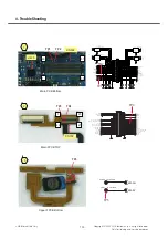
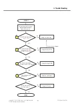
Страница 79: ...8 TP1 is same to 1 8V Finish TP1 TP2 TP2 TP1 U 2 2 3 0 6 C 7 0 6 C U 1 0 S B 2 0 1 1 P S I 3 0 6 U 7 6 5 4 8 3 9 2 0 1 1 11 12 13 14 15 PGND SOFTCON VPU_3_3 VCC_5_0 VREG_3_3 E O _ C N V C R D O P V _ P V D VM_VMO SUSPND VCC_IO VBUSDET 1 1 6 C U 1 3 3 5 1 6 R 3 3 8 1 6 R 8 V 1 _ E D D V S U B V K 0 0 1 2 2 6 R M 1 3 2 6 R M 1 5 2 6 R K 5 1 7 2 6 R M V _ T A D _ B S U E O _ B S U P V _ T A D _ B S U...

Страница 80: ...control path DB3150 generates SIM interface signals 1 8V level to AB3000 AB3000 converts SIM interface signals to 3V SIM works well Finish START Yes Reconnect SIM card Resolder S601 on main PCB and check the contact between S601 and SIM card Change main board SIM works well Finish Yes N o N o SIM works well Finish Yes N o Change SIM card Main Board Bottom side S601 ...

Страница 81: ...k or PDA Change main board MicroSD works well Finish Yes No No MicroSD works well Change the MicroSD No Yes Re insert MicroSD Yes No Yes VDDG_2V85 TP1 is same to 2 85V Finish Change Main board Yes No APP_GP_MMC_DET TP2 is same to 0 V Change Main board TP1 TP2 100K R632 8 V 1 _ E D D V 3 0 6 D Z R 2 T S C 8 6 B S R S601 49448 1611 ENSY0018601 16 15 14 13 12 11 21 0 1 9 8 7 6 5 4 3 2 1 7 1 8 1 2 T S...

Страница 82: ... 1 Key Trouble y Trouble Key works well START Yes Press the key button No Change the key FPCB Finish Change Main Board Check key button If Key button is pressed or appearance is abnormal Change the key button works well Yes Finish No Check BtoB connector CN100 Re assemble CN100 Check connector soldering Re solder CN100 works well Yes Finish No works well Yes Finish No 1 2 ...

Страница 83: ...100 Check connector soldering Re solder CN100 2 CN100 T A B V 4 2 1 4 2 6 T X A 0 0 1 N C 3 1 2 1 4 1 1 1 5 1 0 1 6 1 9 7 1 8 8 1 7 9 1 6 0 2 5 1 2 4 2 2 3 3 2 2 4 2 1 1 G 2 G 3 G 4 G 8 V 1 _ E D D V N _ A W S N O 5 N I Y E K 4 T U O Y E K 3 T U O Y E K 2 T U O Y E K 1 T U O Y E K 0 T U O Y E K 0 N I Y E K 1 N I Y E K 2 N I Y E K 3 N I Y E K 4 N I Y E K E S N E S P I L F _ P G _ C C A 1 D E L _ N ...

Страница 84: ... Camera control signals are generated by DB3150 with ISP 4 6 1 3M Camera START Press END Key to turn on the power Is the circuit powered Reconnect the 3M 24pin B to B connector 3M Camera s Operation is OK Change 3M Camera Follow the Power On Trouble Shooting YES NO YES 3M Camera Works NO Change U503 YES NO C510 TP2 2 8V C516 TP1 1 8V 1 2 Change Main Board ...

Страница 85: ...CN501 1 Main Board Bottom side Main Board Bottom side 2 TP 1 TP 2 TP2 TP1 U503 0 1 5 C U 1 U 1 6 1 5 C 8 V 1 _ M A C _ D D V T A B V 3 0 5 U 1 0 0 9 1 3 0 Y S U E W Q P G M 1 1 0 9 T R 9 5 4 6 3 7 2 8 1 N I V 1 T U O V 1 N E 2 T U O V 2 N E 2 C N 1 C N D N G PGND 8 V 2 _ M A C _ D D V 9 1 5 C U 1 N E _ O D L _ M A C _ P G _ P P A TP1 TP2 ...

Страница 86: ...urn on the power Is the circuit powered Reconnect the VGA 20pin socket connector VGA Camera s Operation is OK Follow the Power On Trouble Shooting YES NO VGA Camera Works YES C100 2 8V C101 1 8V 1 Change Main Board NO Change Upper FPCB Pin 15 TP6 of CN702 2 8V Pin 14 TP5 of CN702 1 8V NO Change Main FPCB Change U503 NO 2 3 4 Change VGA Camera NO YES C516 TP3 1 8V C510 TP4 2 8V ...

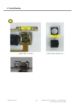
Страница 87: ... 88 LGE Internal Use Only Copyright 2009 LG Electronics Inc All right reserved Only for training and service purposes 4 Trouble Shooting 1 Pin 1 Pin 1 Upper FPCB Top side VGA Camera Socket Cover ...

Страница 88: ...ouble Shooting Main Board Bottom side 2 TP 3 TP 4 TP4 TP3 U503 0 1 5 C U 1 U 1 6 1 5 C 8 V 1 _ M A C _ D D V T A B V 3 0 5 U 1 0 0 9 1 3 0 Y S U E W Q P G M 1 1 0 9 T R 9 5 4 6 3 7 2 8 1 N I V 1 T U O V 1 N E 2 T U O V 2 N E 2 C N 1 C N D N G PGND 8 V 2 _ M A C _ D D V 9 1 5 C U 1 N E _ O D L _ M A C _ P G _ P P A TP3 TP4 ...

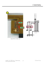
Страница 89: ... training and service purposes 4 Trouble Shooting 21 20 1 40 Main FPCB Top side 3 TP 5 TP 6 TP 5 TP 6 9 1 8 1 7 1 6 1 5 1 4 1 4 2 1 0 4 6 T X A 0 2 3 G 4 G 8 V 1 _ M A C _ D D V 8 V 2 _ M A C _ D D V A D S _ C 2 I _ P P A L C S _ C 2 I _ P P A N S E R _ I C 2 O C C C N Y S H _ I C TP5 TP6 ...

Страница 90: ...eserved Only for training and service purposes LGE Internal Use Only 4 Trouble Shooting 4 Upper FPCB Bottom side TP 7 TP 8 TP7 TP8 u 1 0 0 0 1 C 16 17 18 19 20 3 D N G P 4 D N G P AVDD IOVDD RESET SCL SDA VDD_CAM_2V8 VDD_CAM_1V8 u 1 0 1 0 1 C TP7 TP8 ...

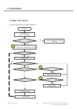
Страница 91: ...ls are generated by DB3150 START Press END Key to turn on the power Is the circuit powered Reconnect the LCD FPCB 37pin CN701 LCD s Operation is OK Follow the Power On Trouble Shooting YES NO LCD Works YES 1 Change Main Board LCD display OK Change U502 NO Change LCD NO YES Is the backlight on C703 TP1 3 2V NO NO C514 TP2 2 8V Change Main FPCB NO LCD s Operation is OK 2 3 NO ...

Страница 92: ... 93 Copyright 2009 LG Electronics Inc All right reserved Only for training and service purposes LGE Internal Use Only 4 Trouble Shooting 1 LCD Bottom side Main FPCB Top side CN701 ...

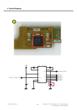
Страница 93: ...01 2 5 1 1 0 1 4 1 3 1 3 2 1 1 1 9 6 8 5 7 4 1 T O F I 9 6 1 3 T A A 1 0 1 U 1 C 2 C 1 C 2 C P C T U O N I 1 D 2 D T E S _ N E 3 D 4 D D N G 5 D D N G P 6 D T A B V u 0 1 0 0 7 C 3 0 7 C u 0 1 u 1 1 0 7 C u 1 2 0 7 C 5 L B _ D C L 1 L B _ D C L 3 L B _ D C L 2 L B _ D C L 4 L B _ D C L L R T C _ L B _ D C L _ P G _ P P A T H G I L K C A B _ D D V TP1 ...

Страница 94: ...r training and service purposes LGE Internal Use Only 4 Trouble Shooting TP 2 TP2 U502 u 1 4 1 5 C u 1 6 0 5 C 1 0 7 5 5 3 0 Y S U E F R T D 1 8 2 K 3 0 1 P R 2 0 5 U 5 2 3 1 4 T U O V D D V D N G E C PGND 8 V 1 _ E D D V T A B V 8 V 2 _ D C L _ D D V 100K R505 TP2 ...

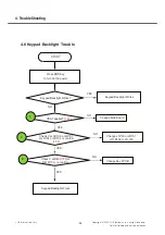
Страница 95: ...klight Trouble START Press END Key to turn on the power Keypad Backlight Works YES NO VBAT applied TP1 Change Main Board NO Check V at LD100 or LD101 or LD102 or LD103 is confirm TP2 NO Change LD100 or LD101 Of LD102 or LD 103 YES YES YES Keypad Backlight Works Check V at R401 TP3 or R410 TP4 is confirm NO Change Key FPCB 1 1 2 Keypad Backlight Works ...

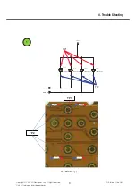
Страница 96: ...ining and service purposes LGE Internal Use Only 4 Trouble Shooting TP1 TP2 TP1 Key FPCB Top TP2 1 Z A A 7 4 S B B E L 1 0 1 D L Z A A 7 4 S B B E L 3 0 1 D L Z A A 7 4 S B B E L 0 0 1 D L Z A A 7 4 S B B E L 2 0 1 D L T A B V 1 D E L _ N I A M 2 D E L _ N I A M TP1 TP2 ...

Страница 97: ...nc All right reserved Only for training and service purposes 4 Trouble Shooting 2 TP3 TP4 Main board Bottom CN503 100 R401 100 R410 H10 H12 B6 B7 D6 A6 L12 SLEEPB LED1 LED2 LED3 VIBR SDA SCL SHARED_I2C_SDA SHARED_I2C_SCL APP_SLEEP MAIN_LED2 MAIN_LED1 MOTOR_EN ...

Страница 98: ...ing 4 9 1 Receiver 4 9 Audio Trouble Shooting Signals to the receiver Receiver signals are generated at AB3000 BEARP BEARN Receiver path 1 AB3000 BEARP BEARN 2 CN502 on main board 3 Main FPCB 4 Upper FPCB 5 Receiver Note It is recommended that engineer should check the soldering of R L C along the corresponding path before every step ...

Страница 99: ...3 8 2 9 1 1 A _ T U O N I 1 B _ T U O N I 2 A _ T U O N I 2 B _ T U O N I 3 A _ T U O N I 3 B _ T U O N I 4 A _ T U O N I 4 B _ T U O N I G1 G2 8 V 2 _ D C L _ D D V 100K R507 0 0 8 1 1 N S 2 8 1 D H 5 1 M L B 3 0 5 B F 0 0 8 1 1 N S 2 8 1 D H 5 1 M L B 5 0 5 B F 1 5 4 0 5 R A D S _ C 2 I _ P P A L C S _ C 2 I _ P P A K L C P _ I C N D S _ A G V _ P G _ C C A 0 K L C S Y S L C S _ M _ D E L _ P G ...

Страница 100: ...t Does the sine wave appear at TP1 TP2 Change the main board Does the sine wave appear at Number TP3 TP4 in the main FPCB CN702 Change the Main FPCB Does the sine wave appear at EAR PAD TP5 in Upper FPCB Change the Upper FPCB Is the soldering of the receiver OK Resolder the Receiver Can you hear sine wave out of the receiver Change the Receiver END YES YES YES YES YES NO NO NO NO NO 1 2 3 3 The si...

Страница 101: ...02 LGE Internal Use Only Copyright 2009 LG Electronics Inc All right reserved Only for training and service purposes 4 Trouble Shooting Measured 1khz Sine Wave Signal 1 3 2 Measured 1khz Sine Wave Signal ...

Страница 102: ...di MP3 Key Tone Signals to the speaker Speaker signals are generated at AB3000 SPKRP SPKRN Speaker path 1 AB3000 SPKRP SPKRN 2 C466 C467 on the main board 3 U405 audio amp on the main board 4 VA501 VA502 on the main board 5 CN100 on the Key FPCB 6 Speaker Note It is recommanded that engineer should check the soldering of R L C along the corresponding path before every step ...

Страница 103: ... 5 0 4 U C4 D3 4 B 4 D 3 C 3 B 5 B 2 B 5 D 2 C 1 C 2 D 1 D 2 A 1 A 5 A 4 A C5 B1 A3 VSS VDD PVDD N 1 C P 1 C R P H L P H 2 A N I 1 A N I 2 B N I 1 B N I T U O S A I B T U O A D S L C S N I X R N I X R GND PGND C460 1UF 8 6 4 C F U 1 F u 8 1 0 0 7 6 4 C 0 7 4 C F p 0 2 1 F u 8 1 0 0 6 6 4 C P K P S L N K P S L P R K P S N R K P S L _ R A E R _ R A E R _ R A E _ S H L _ R A E _ S H L C S _ M F _ P G...

Страница 104: ...Hz tone out Does the sine wave appear at C467 TP1 C466 TP2 Change the main board Does the sine wave appear at C470 TP3 C469 TP4 Change the U405 YES YES NO NO Can you hear sine wave out of a speaker Change each Speaker END YES NO 1 1 The sine wave not appear Does the sine wave appear at EAR PAD TP5 in Upper FPCB Change the KEY FPCB Is the soldering of the speaker OK Resolder the Speaker YES YES NO ...

Страница 105: ... 106 LGE Internal Use Only Copyright 2009 LG Electronics Inc All right reserved Only for training and service purposes 4 Trouble Shooting Measured 1khz Sine Wave Signal 3 ...

Страница 106: ...eo Recorder Microphone Signal Flow MIC is enable by MIC Bias CCO1 MIC1P MIC1N signals to AB3000 CCO2 MIC4P MIC4N signals to AB3000 Check Points Microphone bias Audio signal level of the microphone Soldering of components Signal from the mic1 MIC1 CN100 on KEY FPCB CN521 522 on main board AB3000 Signal from the mic2 MIC C705 706 on Upper FPCB FB102 103 on Upper FPCB CN700 on Main FPCB FB503 505 on ...

Страница 107: ... 108 LGE Internal Use Only Copyright 2009 LG Electronics Inc All right reserved Only for training and service purposes 4 Trouble Shooting 1 MIC1 MIC2 2 ...

Страница 108: ...9 LG Electronics Inc All right reserved Only for training and service purposes LGE Internal Use Only 4 Trouble Shooting START Change the MIC Does it work properly END Yes Yes No Does not open Tx path about Mic No Yes 1 2 ...

Страница 109: ...splay on the main LCD Can you hear sine wave out of the receiver END YES YES NO NO NO Does the sine wave appear at C462 TP3 C463 TP4 Resolder CN601 Pins or change the Headset Does the sine wave appear at C464 TP1 C465 TP2 1 YES Change the main B d YES NO Does the sine wave appear at FB602 TP6 FB603 TP7 NO 4 9 4 Headset Receiver Voice call Video Telephony MP3 Change the main B d Change the main B d...

Страница 110: ...rt Headset Does the Headset icon display on the main LCD YES Does it work properly Try again from the start END YES YES NO NO Change the main B d Check the signal level at FB603 TP5 at the putting Audio signal in MIC Resolder FB603 TP5 and try again If fail again Change the main B d A few hundred of mV Of the signal measured at FB603 TP5 2 4 9 5 Headset MIC Voice call Video Telephony NO change the...

Страница 111: ...R A E R _ R A E _ S H L _ R A E _ S H L C S _ M F _ P G _ P P A A D S _ M F _ P G _ P P A TP1 TP2 TP4 TP3 n 0 7 2 1 0 6 L u 2 2 5 2 6 C K 1 0 4 6 R 0 1 5 3 6 R K 5 1 9 3 6 R 0 1 6 3 6 R I N D 4 2 6 C 0 0 8 1 1 0 6 B F 1 N S 2 8 1 D H 5 1 M L B 1 N S 2 8 1 D H 5 1 M L B 0 0 8 1 2 0 6 B F C P 5 2 4 0 S 8 1 J E S H 1 0 6 N C 0 2 8 1 7 1 6 1 5 1 4 1 3 1 2 1 1 1 0 1 9 8 7 6 5 4 3 2 1 9 1 3 0 6 B F 1 N ...

Страница 112: ...E_RTK 2 0 4 D 1 3 2 A2 A1_C2 C1 7 1 4 R K 7 4 2 0 4 Q J D 1 1 9 A I S 1 G 1 S 1 D 3 D 4 D 2 D 2 G 2 S F P 5 _ 2 1 _ 5 1 3 M C 1 0 4 X z H K 8 6 7 2 3 2 1 5 2 4 C u 3 3 R424 300K KQ03LP 3R CN402 3 2 1 D1 D2 2 3 4 R M 0 0 1 3 3 4 R M 5 2 1 J 3 F 2 E 2 F 1 E 1 H 1 1 G 2 1 G 4 H 3 K 3 J 2 K 0 1 G 2 1 J 1 1 K 2 1 K 1 L A T X 2 L A T X Z H K 2 3 N _ F F O M I S N _ T S R S K L C S T A D S A T A D B E S ...

Страница 113: ...nnect terminals of I O connector Connection OK Change I O connector NO YES Change Main board NO YES Is it charging properly END YES NO Change Main board 1 2 3 start connector Connection OK Change I O connector NO YES Is the DCIN voltage TP3 5 0V NO YES after changing Q402 TP4 END NO 2 3 Trouble Shooting Charging YES YES Is the TA voltage TP2 5 0V Change TA NO Change TA NO 3 4 ...

Страница 114: ...34 N I C D 0 2 1 J 1 N S 1 2 1 G P 8 1 M L B 5 0 6 B F 8 0 6 C U 1 T A B V S U B V n 0 0 1 7 1 6 C 1 2 6 C p 0 9 3 2 2 6 C p 0 9 3 p 0 9 3 3 2 6 C H S A L F P P V N _ B W S N O X T _ T R A U _ C C A _ P P A X R _ T R A U _ C C A _ P P A S U B V N I C D TP3 TP2 TP1 0 3 S 1 2 5 B R 4 0 4 D 1 0 4 D Z B 6 _ 5 1 6 E T Z D E T A B V 3 1 4 R 0 7 1 4 R K 7 4 2 0 4 Q J D 1 1 9 A I S 1 G 1 S 1 D 3 D 4 D 2 D...

Страница 115: ...xamined 4 11 1 Bluetooth Power path start 1 Check BT IC Block TP1 1 8V TP2 2 75V 1 Go to 4 11 2 OK NG Check AB3000 U300 Main PCB TOP TP1 TP2 1 0603 0 1 2 C u 1 0 6 L 5 L 4 L 8 F 7 F 4 D 6 E 7 N 4 J 2 M 2 C 1 C 8 M 3 C 2 B 1 L C _ R V S R _ T B 2 L C _ R V S R _ T B D _ R V S R _ T B M S D _ R V S R _ T B N _ R V S R _ T B F R _ R V S R _ T B L R T C _ G E R _ T B D V H _ T B D L C _ D D V _ T B 1 ...

Страница 116: ...th start 1 Check BT_CLK Buffered MCLK TP1 26MHz 2 Check MCLKSEC TP2 26MHz 1 Go to 4 11 3 OK NG Replace U107 OK NG Check RF3000 U102 Main PCB TOP TP2 TP1 1 R101 0 u 7 4 0 2 1 C 1 2 1 C u 1 0 8 V 1 _ E D D V 5 1 1 R 3 3 3 0 6 0 100K R119 R L R D 5 2 1 G 1 C V L 4 7 N S 7 0 1 U 4 3 2 5 1 E O _ C C V A D N G Y K L C _ T B N _ Q E R K L C _ T B K L C M 3 0 6 0 TP2 TP1 ...

Страница 117: ...Power level at BT IC Output C215 with Spectrum Analyzer TP1 Range 0 4dBm No Yes Replace BT Chip U201 Replace ANT201 start TP1 TP1 F R _ T B _ S S V 1 C 3 4 0 7 T B 0 5 4 2 1 2 A E D 1 0 2 L F 6 3 2 4 1 5 P B _ U 1 P B C D _ P B 2 P B G1 G2 7 5 L F H 0 5 4 2 S C A 1 0 2 T N A D E E F Y M M U D F R _ T B _ S S V F R _ T B _ S S V 1 5n L202 I N D 4 1 2 C p 2 1 5 1 2 C TP1 ...

Страница 118: ...d Top side X101 U102 Reference Description Reference Description IS101 WCDMA Isolater FL101 WCDMA Duplexer U104 DCDC Converter U105 GSM PAM with ASM N101 Directional Coupler U103 Power Detector U101 WCDMA BC 1 PAM FL104 PCS Rx SAW Filter U101 WCDMA BC 1 PAM FL104 PCS Rx SAW Filter FL103 WCDMA BC 1 Tx Filter FL105 GSM Rx SAW Filter FL102 WCDMA BC 1 Rx Filter FL106 DCS Rx SAW Filter U106 WCDMA Trans...

Страница 119: ...uble Shooting 4 13 Procedure to check start Oscilloscope setting 1 Check Power Source Block 2 Check VCXO Block Agilent 8960 Test mode WCDMA Ch 9750 Uplink Ch 10700 Downlink 4 Check WCDMA Block Agilent 8960 Test mode GSM Ch 190 P L 7 level setting Ch 190 60dBm setting 5 Check GSM Block Redownload SW Cal 3 Check Ant SW Module ...

Страница 120: ...s Inc All right reserved Only for training and service purposes LGE Internal Use Only 4 Trouble Shooting 4 14 Checking Common Power Source Block Step 2 GSM PAM Block Step 3 WCDMA PAM Block GSM PA VBAT WCDMA DC DC VBAT WCDMA DC DC VBAT ...

Страница 121: ...side Power Source Block g Main Board Top side Step 1 VBAT Block c TP5 TP1 TP2 TP3 TP4 p 2 2 1 0 4 C T A B V T A B V KDS221E_RTK 2 0 4 D 1 3 2 A2 A1_C2 C1 5 2 4 C u 3 3 R424 300K KQ03LP 3R CN402 3 2 1 D1 D2 3 4 R M 5 2 p 2 2 2 4 4 C p 2 2 3 4 4 C W 4 1 h t a p n r u t e r n n o C y r e t t a B D N G _ T T A B 1 2 1 0 2 Close to Pin 1 d n u o r g e n o h P TP3 TP1 TP2 TP4 ...

Страница 122: ...n Power Source Block g To Check Power source to Check if main power source input or not Yes No Proceed to the Step 2 3 7V OK No Yes Check the Power Supply Short No Yes Soldering Check Component CN300 In Power Source Block g Check Point TP2 in Power Source Block g To Check Power source Change Board Check TP1 TP2 in Block c g to check inner line connection From TP4 to TP3 ...

Страница 123: ...IN GND1 GND2 GND3 GND4 OUT 5 0 1 U 9 1 5 7 7 Y K S 9 2 5 1 6 1 4 1 7 1 3 1 8 1 2 1 9 1 1 1 0 2 9 2 2 4 2 0 1 7 1 2 6 5 3 2 4 5 2 3 2 6 2 1 7 2 8 8 2 T N A 1 S B 2 S B N E X T E D O M T T A B V D V S R C P A V 4 X R 3 X R N I _ M S G 2 X R 1 X R N I _ S C P _ S C D 1 A M D C W 3 1 D N G 1 D N G 2 1 D N G 2 D N G 1 1 D N G 3 D N G 0 1 D N G 4 D N G 9 D N G 5 D N G 8 D N G 7 D N G D N G P 6 D N G 2 4...

Страница 124: ...in GSM PAM Block d to Check if main power source input or not Check TP1 TP3 TP4 TP5 in Block c g to check inner line connection From TP1 to TP3 TP4 TP5 Check Point TP1 in Power Source Block g To Check Power source 3 7V OK Yes No Proceed to the Step 3 3 7V OK No Yes Check the Power Supply Short No Yes Soldering Check Component CN300 In Power Source Block g Change Board ...

Страница 125: ...ce Block g TP4 TP5 TP3 Step 3 WCDMA PAM Block e 3 7V OK Step 3 Check VBAT TP3 in WCDMA PAM Block e Yes No See the Next Page 3 7V OK No Yes Check the Power Supply Short No Yes Soldering Check Component CN300 In Power Source Block g Check Point TP1 in Power Source Block g To Check Power source Change Board Check TP1 TP3 in Block e g to check inner line connection From TP3 to TP1 TP1 TP2 ...

Страница 126: ... Next Part Check Point VRADA_2V8 TP1 AB3000 AB3000 TP1 TP2 5 7 V 2 _ K D D V 8 0 4 R 0 0 9 0 4 R 5 7 V 2 _ H D D V 8 V 2 _ A D A R V 2 1 4 C u 2 2 8 V 1 _ D A R G I D V 4 1 4 C u 1 T A B V 5 8 V 2 _ G D D V 9 1 4 R 0 8 V 1 _ E D D V 0 3 2 4 R 5 V 1 _ D D D V 5 V 2 _ F D D V 4 3 4 R 0 u 1 6 3 4 C 2 1 B 1 1 A 2 1 D 2 1 F 1 1 B 2 1 C A _ D D V O D L T X E D _ D D V E _ D D V C _ D D V H _ D D V 5 6 V...

Страница 127: ...VCXO Block The reference frequency 26MHz from U102 Transceiver RF3000 is used WCDMA TX part and BB part Bluetooth part Therefore 3 test points in the following figure should be checked Phone Oscilloscope Notebook to send TP command Connection for Checking VCXO Block U102 Transceiver X100 Crystal RF3000 Main board Top side U302 Digital Base Band DB3150 ...

Страница 128: ...Crystal and RF3000 Transceiver part If you already check this crystal part you can skip check 1 Test Point Crystal Part Schematic Crystal Part Figure 4 15 26MHz at TP1 TP1 TP1 3 0 6 0 K 0 0 1 4 0 1 R 8 1 1 R 3 0 6 0 K 0 0 1 0603 100K R120 z H M 6 2 2 6 5 6 2 4 N T 1 0 1 X 2 1 3 4 2 D N G 2 T O H 1 T O H 1 D N G K L C M TP1 Schematic Crystal Part ...

Страница 129: ...TP1 TP1 Figure 4 15 1 Test point 26MHz at BB part Test Point Crystal Part R101 0 u 7 4 0 2 1 C 1 2 1 C u 1 0 8 V 1 _ E D D V 5 1 1 R 3 3 3 0 6 0 100K R119 R L R D 5 2 1 G 1 C V L 4 7 N S 7 0 1 U 4 3 2 5 1 E O _ C C V A D N G Y K L C _ T B N _ Q E R K L C _ T B K L C M 3 0 6 0 TP1 P T 8 0 3 P T P T 5 0 3 P T 8 1 V 1 1 P 6 1 W 5 1 Y 6 1 Y 4 1 W K L C M 0 K L C S Y S 1 K L C S Y S 2 K L C S Y S N _ T...

Страница 130: ...ll right reserved Only for training and service purposes LGE Internal Use Only 4 Trouble Shooting Check TP1 No Refer to Figure 4 15 Yes VCXO part has a problem Changing XTAL or U111 Checking 1 3 26MHz at VCXO VCXO part is O K Check next stage ...

Страница 131: ...e Block Figure 4 16 Front End Module Block Top Antenna Switch Module GSM EDGE PA TP1 TP2 TP3 TP1 TP2 TP3 3 0 6 0 p 2 2 4 1 1 C 5 1 1 C 3 0 6 0 p 2 2 9 1 1 C 3 0 6 0 p 2 2 5 0 1 U 9 1 5 7 7 Y K S 1 2 3 2 5 2 6 2 7 2 8 2 1 S B 2 S B T T A B V C P A V N I _ M S G N I _ S C P _ S C D 0 W S T N A 2 W S T N A 1 W S T N A S C P S C D _ X T M S G E _ X T C P A V TP3 TP2 TP1 ...

Страница 132: ...LGE Internal Use Only 4 Trouble Shooting EGSM Tx ANTSW1 ANTSW2 ANTSW3 WCDMA 2100 DCS PCS Tx 4 17 Checking Front End Module Block input logic 4 17 1 Mode Logic by TP Command DCS Rx PCS Rx ANTSW1 ANTSW2 ANTSW3 ANTSW1 ANTSW2 ANTSW3 EGSM Rx ANTSW1 ANTSW2 ANTSW3 ANTSW1 ANTSW2 ANTSW3 ANTSW1 ANTSW2 ANTSW3 ...

Страница 133: ... 134 LGE Internal Use Only Copyright 2009 LG Electronics Inc All right reserved Only for training and service purposes 4 Trouble Shooting Table 4 1 Front End module Logic ...

Страница 134: ...e Checking this part must check common power source through AB3000 part TP Command MODE 0 SWRX 49 3 Open High OK Resoldering Check each mode By TP command Change the Board No No No Yes Yes Yes Check soldering C106 Check Soldering It is necessary to check short condition Using Tester Check 3 capacitors ANTSW0 TP1 ANTSW1 TP2 ANTSW2 TP3 Check ANTSW0 TP1 To check Switch input power source ...

Страница 135: ...erved Only for training and service purposes 4 Trouble Shooting A EGSM Rx mode EGSM Rx MODE 0 SWRX 49 3 EGSM Rx Logic OK See the Next mode EGSM Tx Mode Change the Board No No Yes Yes Figure 4 17 EGSM Rx Mode Try 4 17 part 4 17 part Check OK ANTSW1 ANTSW2 ANTSW3 High High Low ...

Страница 136: ...e Only 4 Trouble Shooting B EGSM Tx mode EGSM Tx MODE 0 SWTX 0 64 255 GSM850 EGSM Tx Logic OK See the Next mode DCS Rx Mode No No Yes Yes Figure 4 17 1 EGSM Tx Mode Try 4 17 part 4 17 part Check OK ANTSW1 High Æ Low ANTSW2 Low ANTSW3 High Change the Board Change U101 ANTSW1 ANTSW2 ANTSW3 No Yes Low High Low High ...

Страница 137: ...served Only for training and service purposes 4 Trouble Shooting C DCS Rx mode DCS Rx MODE 2 SWRX 699 3 DCS Rx Logic OK See the Next mode DCS Tx Mode Change the Board No No Yes Yes Figure 4 17 2 DCS Rx Mode Try 4 17 part 4 17 part Check OK ANTSW1 ANTSW2 ANTSW3 Low High High ...

Страница 138: ...ng and service purposes LGE Internal Use Only 4 Trouble Shooting D PCS Rx mode PCS Rx MODE 1 SWRX 661 3 PCS Rx Logic OK See the Next mode PCS Tx Mode Change the Board No No Yes Yes Figure 4 17 3 PCS Rx Mode Try 4 17 part 4 17 part Check OK ANTSW1 ANTSW2 ANTSW3 High High High ...

Страница 139: ...ly for training and service purposes 4 Trouble Shooting E DCS PCS Tx mode DCS PCS Tx MODE 2 DCS or 1 PCS SWTX 0 699 255 Figure 4 17 4 DCS PCS Tx Mode DCS Tx Logic OK WCDMA1900 Mode Change the Board No No Yes Yes Try 4 17 part 4 17 part Check OK ANTSW1 ANTSW2 ANTSW3 High High Low High ...

Страница 140: ...rnal Use Only 4 Trouble Shooting F WCDMA 2100 mode WCDMA2100 Mode MODE 4 WTXC 9750 1 85 Figure 4 17 5 WCDMA2100 Mode WCDMA2100 Logic OK Change the Board No No Yes Yes Try 4 17 part 4 17 part Check OK ANTSW1 ANTSW2 ANTSW3 Low High Low Input Signal and Power to Front End Module block is OK See the Next Page ...

Страница 141: ...ight reserved Only for training and service purposes 4 Trouble Shooting 4 18 Checking WCDMA Block start 1 Check VCXO Block 4 Check RF TX Level 3 Check Control Signal Re download SW Cal 2 Check Front End Module 6 Check RF RX Level 5 Check PAM Block Figure 4 18 RF BLOCK ...

Страница 142: ... Only 4 Trouble Shooting 4 18 1 Checking VCXO Block Refer to 4 17 4 18 2 Checking Ant SW module Refer to 4 18 4 18 3 Checking Control Signal First of all control signal should be checked data clk strobe Figure 4 18 1 Test points Control Signal TP3 RF_CTRL_CLK TP2 RF_CTRL_DATA TP1 RF_CTRL_STR1 Pin 13 Pin 12 Pin 14 ...

Страница 143: ...atic Control Signal TP1 RF_CTRL_STR1 TP2 RF_CTRL_DATA TP3 RF_CTRL_CLK p 2 8 8 3 1 C 6 0 1 U N H 5 9 1 6 M O _ 0 0 1 3 F R 20 19 18 17 16 15 14 13 12 11 0 1 9 8 7 6 5 1 _ X T 3 C N X T O L C C V A I X T B I X T A Q X T B Q X T VGACTL DATA CLK EN REFIN NC4 RXIA RXIB RXQA RXQB N _ Q _ X T W P _ Q _ X T W N _ I _ X T W P _ I _ X T W K L C W B R T S _ L R T C _ F R A T A D _ L R T C _ F R K L C _ L R T...

Страница 144: ...l is O K Check next stage Download the SW Check TP1 TP2 TP3 Check shape and pk pk level Refer to Figure 4 18 4 Yes No If signal is not OK even after downloading Change the U201 Figure 4 18 4 Control Signal TP Command MODE 4 WTXC 9750 1 754 643 418 568 SYCT 9750 TP1 RF_CTRL_STR1 TP2 RF_CTRL_DATA TP3 RF_CTRL_CLK TP1 RF_CTRL_STR1 TP2 RF_CTRL_DATA TP3 RF_CTRL_CLK ...

Страница 145: ...ght 2009 LG Electronics Inc All right reserved Only for training and service purposes 4 Trouble Shooting 4 18 4 Checking RF TX Level TP1 WBAND 1 PAM Input TP2 RF3100 Output BAND 1 TP4 Ant SW Top side Bottom side TP5 Ant TP3 FEM Output ...

Страница 146: ... 1 C I N D 8 V 2 _ A D A R V 0 0 F 0 A K 5 9 G 1 B E F A S 3 0 1 L F 2 5 1 4 3 3 G N I T U O 1 G 2 G 7 6 5 4 3 2 1 38 39 40 41 PGND VCCTX RF_DAC2 RF_DAC1 X T D N G 1 C N 2 C N 1 _ X T 3 C N X T O L C C V A I X T 1 _ D N A B _ D O M X T W P _ I _ X T W C C V _ A P W S A I B _ A P W 3 0 6 0 3n L115 I N D 9 0 1 C 1n L103 p 5 0 8 5 1 C 1 0 1 W S 3 B R 0 0 6 2 0 3 4 8 M M 2 6 5 4 3 1 IN GND1 GND2 GND3 ...

Страница 147: ...right reserved Only for training and service purposes 4 Trouble Shooting Phone Spectrum Analyzer Notebook to send TP command Figure 4 18 6 Connection for Checking RF TX Level Figure 4 18 8 Output Level at RF3100 Output TP2 Figure 4 18 7 Output Level at PAM Input TP1 ...

Страница 148: ...nc All right reserved Only for training and service purposes LGE Internal Use Only 4 Trouble Shooting Figure 4 18 11 Output Level at TP5 Ant Figure 4 18 10 Output Level at RF test connector TP4 Figure 4 18 9 Output Level at FEM Output TP3 ...

Страница 149: ...D Test of the Agilent 8960 Set the Maximum Power Yes The SW101 has any problem Change the SW101 TP3 About 15dBm Check the power at the TP3 with probe Refer to Figure 4 18 9 No Yes The L103 will be broken Change the L103 TP5 About 19dBm Check the power at the TP5 Ant with probe Refer to Figure 4 18 11 No Yes The U105 has any problem You have to check PAM block TP1 About 6dBm Check the power at the ...

Страница 150: ... training and service purposes LGE Internal Use Only 4 Trouble Shooting WCDMA band1 PAM VCC_PA C133 C110 from DC DC WPAM input C149 Duplexer Output C129 L112 4 18 5 Checking PAM Block Figure 4 18 12 Test points of WCDMA TX PAM block Bias_CTRL C143 C106 DC DC converter ...

Страница 151: ... To Check PAM output WCDMA PAM is OK See the Next page Level 10dBm No Download the SW Calibrate Level 2dBm Check C149 To Check PAM Input level Check the WCDMA RF Tx Chip RF3100 Yes Yes 1 1V at Po_max Check C115 C157 To Check PAM control signal from AB3000 Bias_CTRL Check the RF3100 to WCDMA PAM Signal line 3 4V Check C133 C110 To Check PAM VCC BIAS from DC DC converter VCC_WPA No No No Change the ...

Страница 152: ... the RX path you have to check the pk pk level and the shape of the RX I Q Feed a CW signal at 2142MHz with a power level of 60dBm Figure 4 18 14 RX I Q signal CW 2142MHz Figure 4 18 13 RF3100 WCDMA Transceiver Bottom About 2 MHz Figure 4 18 15 RX I Q signal WRX_Q_P PIN 2 WRX_Q_N PIN 1 WRX_I_N PIN 3 WRX_I_P PIN 4 WRX_I_ P PIN 4 WRX_I_N PIN 3 WRX_Q_P PIN 2 WRX_Q_ N PIN 1 ...

Страница 153: ...de of the Agillent 8960 Feed a CW signal at 1950MHz Set the RX Continuous mode Check the Mean level at PIN 1 PIN 2 PIN 3 PIN 4 With Oscilloscope Refer to Figure 4 18 14 Yes No Check the frequency at PIN 1 PIN 2 PIN 3 PIN 4 With Oscilloscope Refer to Figure 4 18 15 Yes No Verify whether the signal was similar as Figure 4 18 15 with Oscilloscope Yes No About 160mV About 2MHz Similar Check Next Stage...

Страница 154: ...r training and service purposes LGE Internal Use Only 4 Trouble Shooting 4 19 Checking GSM Block start 2 Check VCXO Block 5 Check RF TX Path 4 Check Control Signal Re download SW Cal 3 Check FEM Module 6 Check RF RX Path 1 Check VRAD_2V8 Figure 4 19 GSM Block Bottom ...

Страница 155: ...e block IF you already check this point while checking power source block 4 14 You can skip this test 4 19 2 Checking VCXO Block Refer to 4 15 Checking VCXO block IF you already check this point while checking VCXO block 4 15 You can skip this test 4 19 3 Checking Front End Module Refer to 4 16 Checking Ant SW Module IF you already check this point while checking Ant SW module 4 16 You can skip th...

Страница 156: ...GE Internal Use Only 4 Trouble Shooting 4 19 4 Checking Control Signal Test Program Script MODE 3 SWTX 190 7 1024 1 STRB STRB CLK CLK DATA DATA Figure 4 19 2 GSM RF Control signal Figure 4 19 1 Test points of RF control signals RF_CTRL_ST RB PIN 6 RF_CTRL_CL K PIN8 RF_CTRL_DA TA PIN7 GSM PAM RF3000 ...

Страница 157: ...ight reserved Only for training and service purposes 4 Trouble Shooting Similar Check PIN6 PIN7 PIN8 of RF3000 Check if there is any Major difference Refer to Figure 4 19 2 Yes No Re download SW Short Yes No Change the board Control signal is OK See next page to check ...

Страница 158: ...ght 2009 LG Electronics Inc All right reserved Only for training and service purposes LGE Internal Use Only 4 Trouble Shooting 4 19 5 Checking RF Tx Path A GSM Tx path Level Figure 4 19 3 GSM DCS PCS Tx Path Level ...

Страница 159: ... Internal Use Only Copyright 2009 LG Electronics Inc All right reserved Only for training and service purposes 4 Trouble Shooting Figure 4 19 4 Test Points of GSM850 EGSM DCS PCS Tx Path Bottom PIN 6 7 8 9 Top ...

Страница 160: ...there is any Major difference Refer to Figure 4 19 5 EGSM 32dBm DCS 29dBm PCS 29dBm No See Next page to check Tx path Similar Yes EGSM DCS PCS Tx path OK See Chapter 4 19 to check Rx path v Agilent 8960 Setting GSM BCH TCH Mode v Oscilloscope Setting 2 DCS Tx MODE 2 SWTX 699 0 1024 1 Test Program Script 3 PCS Tx MODE 1 SWTX 661 0 1024 1 Figure 4 19 5 EGSM DCS PCS Tx Level at 1 EGSM Tx MODE 0 SWTX ...

Страница 161: ... purposes 4 Trouble Shooting C GSM RF Transceiver Check Vapc PIN 25 GSM Tx R124 ྙ DCS PCS Tx R123 ྙ GSM Tx R124 RF3000 U102 Check GSM RF Transceiver No Figure 4 19 6 EGSM DCS PCS Transceiver RF3000 EGSM DCS PCS 5dBm See Next page to check Tx path Check GSM RF Transceiver Output power at ᐭ No Yes Redownload SW ...

Страница 162: ...PCS 29 5dBm Yes Changing GSM PAM U105 Check EGSM DCS PCS PAM output power at SW101 GSM Tx path OK See Next page to check Check Vapc level Check if there is any Major difference Refer to Figure 4 19 7 Yes No Redownload SW Cal EGSM 1 5 V No Figure 4 19 7 Test points of EGSM DCS PCS Tx DCS PCS 1 3 V EGSM DCS PC S Tx L115 C158 Bottom GSM EDG E PAM Ant SW U105 Vapc PIN 25 Top ...

Страница 163: ... LG Electronics Inc All right reserved Only for training and service purposes 4 Trouble Shooting 4 19 6 Checking RF Rx Path A GSM Rx path Level Figure 4 19 8 GSM DCS PCS Rx Path Level EGSM 50dBm DCS 50dBm PCS 50dBM EGSM 51 5dBm DCS PCS 51 7dBm ...

Страница 164: ...WRX 2 700 0 1024 1 DCS SWRX 1 700 0 1024 1 PCS Test Program Script 1 EGSM Rx SWRX 0 65 5 1024 1 EGSM v Agilent 8960 Setting CW Mode EGSM 50dBm Ch65 948MHz DCS 50dBm Ch700 1842 8MHz PCS 50dBm ch700 1967 8MHz v Oscilloscope Setting Figure 4 19 9 Test Points of GSM DCS PCS Rx Bottom GSM Transceiver RF3000 U102 GSM EDG E PAM U105 DCS Rx PCS Rx EGSM Rx Top ...

Страница 165: ...Level Check GSM Rx path OK Check EGSM DCS PCS Rx signal level at Yes EGSM 51 5dBm DCS PCS 51 7dBm Change Ant SW module U105 No Figure 4 19 10 EGSM DCS PCS Rx path v Agilent 8960 Setting CW Mode EGSM 50dBm Ch65 948MHz DCS 50dBm Ch700 1842 8MHz PCS 50dBm ch700 1967 8MHz Bottom GSM Transceiver RF3000 U102 GSM EDG E PAM U105 Top DCS Rx PCS Rx EGSM Rx ...

Страница 166: ... CXC1723914_B2_P1A ldr CXC1723915_B2_P1A ldr CXC1723918_B2_P1A_ACC_Production_dev ldr CXC1723919_1B2_P1A_APP_Large_Production_dev ldr C DOWNLOAD Model EMP GR500 GR500_081201_MP dll Model DLL SSW File Model Binary MAP File GDFS Files 2 Frame Preference Dialog Port Selection Select download ports DLL Selection Select Model DLL Download Configuration Setup DLL configuration DLL Information Show DLL c...

Страница 167: ...page is depend on model DLL To run press Download Configuration at Frame Preference Dialog Use USB Address If this check is unchecked Connected phone use from Port 1 dialog Unchcked use fixed USB port You should assign port number with USB Address Image Files Select Image binary files GDFS File Select GDFS files GD580 GD580 GD580 GD580 GD580 GD580 GD580 GD580 ...

Страница 168: ...og and select Start Button on main page Connect phone and wait until download finished Usage fixed USB port 1 How to run Not Qualcomm USB Driver but EMP USB Driver assign port ID in order phone connected from ID 1 For use fixed port ID assign port ID before download job 2 Setting Phone should connect just one before detect USB address Connect phone first curl cord Press Set Button Check USB Addres...

Страница 169: ...Use Only Copyright 2009 LG Electronics Inc All right reserved Only for training and service purposes 6 Block Diagram 6 1 System Block Diagram Figure 6 1 GD580 Block Diagram 6 Block diagram Figure 6 1 GD580 Block Diagram ...

Страница 170: ...Copyright 2009 LG Electronics Inc All right reserved Only for training and service purposes LGE Internal Use Only 6 Block Diagram 6 2 RF Block Diagram Figure 6 2 RF Block Diagram Figure 6 2 RF Block Diagram ...

Страница 171: ...Internal Use Only Copyright 2009 LG Electronics Inc All right reserved Only for training and service purposes 6 Block Diagram 6 3 Power Block Diagram Figure 6 3 Power Block Diagram Figure 6 3 Power Block Diagram ...

Страница 172: ...l right reserved Only for training and service purposes LGE Internal Use Only 6 Block Diagram 6 4 Control Signals and Clocks Block Diagram Figure 6 4 Control Signals and Clocks Block Diagram Figure 6 4 Control Signals and Clocks Block Diagram ...

Страница 173: ...al Use Only Copyright 2009 LG Electronics Inc All right reserved Only for training and service purposes 6 Block Diagram 6 5 Bluetooth Block Diagram Figure 6 5 Bluetooth Block Diagram Figure 6 5 Bluetooth Block Diagram ...

Страница 174: ...ght 2009 LG Electronics Inc All right reserved Only for training and service purposes LGE Internal Use Only 6 Block Diagram 6 6 Camera Block Diagram Figure 6 6 Camera Block Diagram Figure 6 6 Camera Block Diagram ...

Страница 175: ...GE Internal Use Only Copyright 2009 LG Electronics Inc All right reserved Only for training and service purposes 6 7 LCD Block Diagram Figure 6 7 LCD Block Diagram Figure 6 7 LCD Block Diagram 6 Block Diagram ...

Страница 176: ...09 LG Electronics Inc All right reserved Only for training and service purposes LGE Internal Use Only 6 8 Audio part Block Diagram Figure 6 8 Audio part Block Diagram Figure 6 8 Audio part Block Diagram 6 Block Diagram ...

Страница 177: ...ight 2009 LG Electronics Inc All right reserved Only for training and service purposes 6 9 Memory Micro SD USIM Block Diagram Figure 6 9 Memory Micro SD USIM Block Diagram Figure 6 9 Memory Micro SD USIM Block Diagram 6 Block Diagram ...

Страница 178: ...LG Electronics Inc All right reserved Only for training and service purposes LGE Internal Use Only 6 10 USB Transceiver for Full Speed Block Diagram 6 Block Diagram Figure 6 10 USB Transceiver for Full Speed Block Diagram ...

Страница 179: ... 180 LGE Internal Use Only Copyright 2009 LG Electronics Inc All right reserved Only for training and service purposes ...
Страница 180: ...XEN MODE VBATT RSVD VAPC RX4 RX3 GSM_IN RX2 RX1 DCS_PCS_IN WCDMA1 GND13 GND1 GND12 GND2 GND11 GND3 GND10 GND4 GND9 GND5 GND8 GND7 PGND GND6 R115 33 VRADA_2V8 L111 10n 8 2p C138 DNI C139 10u C143 L112 DNI VDIGRAD_1V8 C141 10u C142 10u 10u C140 0603 10n C131 0603 22p C145 4 7u C146 5 6p C147 5 6n L113 VDIGRAD_1V8 VCC_PA C149 56p 56p C123 0 5p C122 1 5n L102 SAFEB2G14FA0F00 FL102 4 5 1 3 2 G1 O1 IN G...

Страница 181: ...PIO_9 BT_VSSDIG1 BT_GPIO_11 BT_VSSDIG2 BT_GPIO_10 BT_VSSDIG3 BT_GPIO_16 BT_VSSDIG4 BT_GPIO_8 BT_VSSDIG5 BT_VSSANA1 BT_GPIO_0 BT_VSSANA2 BT_CLK_REQ_IN_1 BT_VSSANA3 BT_CLK_REQ_IN_2 BT_VSSANA4 BT_HOST_WAKEUP BT_VSSANA5 BT_VSSANA6 BT_CONFIG_1 BT_VSSANA7 BT_CONFIG_2 BT_VSSANA8 BT_CONFIG_3 BT_VSSANA9 BT_VSSANA10 BT_CLK_REQ_OUT_2 BT_VSSANA11 BT_VSSANA12 BT_RSVR_CL1 BT_VSSRF1 BT_RSVR_CL2 BT_VSSRF2 BT_RSVR...

Страница 182: ...TEMU1_N EMIF1_D10 EMIF1_D11 ETM_PSTAT0 EMIF1_D12 ETM_PSTAT1 EMIF1_D13 ETM_PSTAT2 EMIF1_D14 ETM_TSYNC EMIF1_D15 ETM_TCLK EMIF1_SDCS_N ETM_TPKT0 EMIF1_SDCLK ETM_TPKT1 EMIF1_SDCKEN ETM_TPKT2 EMIF1_SDCAS_N ETM_TPKT3 EMIF1_SDRAS_N ETM_TPKT4 EMIF1_WE_N ETM_TPKT5 EMIF1_BE0_N ETM_TPKT6 EMIF1_BE1_N ETM_TPKT7 EMIF2_A01 MSACCIRQ_N EMIF2_A02 MSAPPIRQ_N EMIF2_A03 EMIF2_A04 I2S0CLK EMIF2_A05 I2S0WS EMIF2_A06 I2...

Страница 183: ...TH5 VSSTH6 VSSTH7 VSSTH8 VSSTH9 VSSTH10 VSSTH11 VSSTH12 SUB SUB2 VSS_A VSS_B VSS_C VSS_D VSS_DIG VSS_CODEC VSS_BEAR VSS_SPKRP VSS_SPKRN VSS_PLL 5 6 V 2 _ C D D V 5 V 1 _ D D D V 4 2 7 4 4 R u 0 1 2 0 4 L 0 8 3 4 R p 2 2 2 4 4 C 0 9 3 4 R p 2 2 3 4 4 C 39K R442 K 5 1 3 4 4 R F U 1 7 5 4 C 9 6 4 C F p 0 2 1 9 5 4 C F U 1 0 F U 1 1 6 4 C I N D 2 6 4 C 3 6 4 C I N D 8 5 4 C F U 1 F U 1 5 6 4 C T A B V...

Страница 184: ...03 10 5 6 7 8 9 INOUT_A1 1 INOUT_B1 INOUT_A2 2 INOUT_B2 INOUT_A3 3 INOUT_B3 INOUT_A4 4 INOUT_B4 G1 G2 C518 0 1U 1000 FB509 VBAT SFEY0011701 ICVE10184E070R100FR FL504 10 5 6 4 7 3 8 2 9 1 INOUT_A1 INOUT_B1 INOUT_A2 INOUT_B2 INOUT_A3 INOUT_B3 INOUT_A4 INOUT_B4 G1 G2 U503 EUSY0319001 RT9011 MGPQW 9 5 4 6 3 7 2 8 1 VIN VOUT1 EN1 VOUT2 EN2 NC2 NC1 GND PGND VDD_CAM_2V8 C519 1U 0 1U C520 VDD_LCD_2V8 1800...

Страница 185: ...VDDE_1V8 UT 0 1U C612 C613 0 1U C610 4 7U 10K R613 VA601 ICVL0518100Y500FR VBAT 33 R615 R616 DNI 39K R617 ZD603 RSB6 8CST2R VBUS R618 33 C615 DNI VDDE_1V8 R619 47K C616 10n VSMF05LCC D602 4 3 5 2 6 1 VBUS R620 0 UR 3 3K R621 VA602 ICVL0518100Y500FR 100K R622 100n C617 1M R623 VDDE_1V8 390 R624 DNI C618 VDDE_1V8 1M R625 100K R626 S601 49448 1611 ENSY0018601 20 19 16 15 14 13 12 11 21 10 9 8 7 6 5 4...

Страница 186: ...U D 2 1 1 C I N D n 7 4 3 0 1 L R F 0 5 1 V 1 0 1 5 0 5 0 L V C I 0 0 1 A V n 7 4 4 0 1 L n 6 5 7 0 1 L n 7 4 5 0 1 L n 7 4 6 0 1 L 0 0 1 U X V N 1 3 0 2 5 U B 5 2 3 1 4 T U O D D V D N G C N PGND T A B V n 0 0 1 2 0 1 C n 0 0 1 1 0 1 C 8 V 1 _ E D D V Z A A 7 4 S B B E L 1 0 1 D L Z A A 7 4 S B B E L 3 0 1 D L Z A A 7 4 S B B E L 0 0 1 D L Z A A 7 4 S B B E L 2 0 1 D L T A B V P T 1 0 1 P T 4 2 1...

Страница 187: ...31 10 32 9 33 8 34 7 35 6 36 5 37 4 38 3 39 2 40 1 G1 G2 G3 G4 VDD_CAM_1V8 VDD_CAM_2V8 C701 1u 1u C702 APP_I2C_SDA APP_I2C_SDA APP_I2C_SCL APP_I2C_SCL CI_PCLK CI_PCLK ACC_GP_VGA_SDN ACC_GP_VGA_SDN APP_GP_LED_M_SCL APP_GP_LED_M_SCL APP_GP_LED_M_SDA APP_GP_LED_M_SDA ACC_GP_LED_M_LDO_EN ACC_GP_LED_M_LDO_EN LCD_VSYNC LCD_VSYNC LCD_RESN LCD_RESN LCD_CSN LCD_CSN LCD_ADS LCD_ADS LCD_WEN LCD_WEN CI_VSYNC ...

Страница 188: ...C705 47p C704 SPU0410HR5H PB MIC700 4 3 2 1 P G1 G2 O VDD_CAM_2V8 VDD_CAM_1V8 AXM41511LG1 S100 15 14 13 12 11 10 9 8 7 16 6 17 18 19 20 1 2 3 4 5 D0 PCLK GND MCLK DVDD PGND3 PGND4 AVDD PGND2 IOVDD PGND1 RESET SCL D1 SDA D2 D3 PGND5 D4 PGND6 D5 PGND8 PGND7 D6 D7 VSYNC HSYNC STANDBY 47 R100 VDD_CAM_2V8 VDD_CAM_1V8 0 1u C101 VBOOST VBAT VDDE_1V8 APP_I2C_SDA APP_I2C_SDA APP_I2C_SCL APP_I2C_SCL ACC_GP_...

Страница 189: ... 190 LGE Internal Use Only Copyright 2009 LG Electronics Inc All right reserved Only for training and service purposes ...
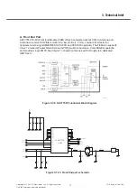
Страница 190: ... 191 Copyright 2009 LG Electronics Inc All right reserved Only for training and service purposes LGE Internal Use Only 8 BGA Pin Map 8 BGA Pin Map 8 1 DB3150 Digital BB NC pin ...

Страница 191: ... 192 LGE Internal Use Only Copyright 2009 LG Electronics Inc All right reserved Only for training and service purposes 8 BGA Pin Map 8 2 AB3000 Analog Baseband NC pin ...

Страница 192: ... 193 Copyright 2009 LG Electronics Inc All right reserved Only for training and service purposes LGE Internal Use Only 8 BGA Pin Map 8 3 MCP 2G NAND 1G SDRAM ...

Страница 193: ... 194 LGE Internal Use Only Copyright 2009 LG Electronics Inc All right reserved Only for training and service purposes 8 BGA Pin Map 8 4 RF3000 GSM Transceiver NC pin ...

Страница 194: ... 195 Copyright 2009 LG Electronics Inc All right reserved Only for training and service purposes LGE Internal Use Only 8 BGA Pin Map 8 5 RF3100 WCDMA Transceiver NC pin ...

Страница 195: ... 196 LGE Internal Use Only Copyright 2009 LG Electronics Inc All right reserved Only for training and service purposes 8 BGA Pin Map 8 6 STLC2593 Bluetooth NC pin ...

Страница 196: ... 0 3 C 8 2 3 C 6 3 1 C 5 0 3 C L101 6 0 1 C 9 0 1 L R432 C141 R102 R106 R107 6 0 1 U L104 9 4 1 C C143 1 0 1 U N101 8 0 1 R 4 0 1 C 1 0 1 S I C118 C137 R117 4 1 1 R C202 0 2 1 C 7 0 2 C 9 1 1 R 5 1 1 R C210 1 0 2 R 1 2 1 C 1 0 2 C 1 0 1 R 7 0 1 U R103 5 0 2 C 6 1 1 R 1 1 1 C 7 0 1 C 0 2 1 R 5 0 1 L C139 C157 5 0 1 R C130 C125 3 0 1 U 1 1 1 R 2 1 1 R 0 4 1 C 1 0 1 L F C142 R123 C209 C204 C203 U201 ...

Страница 197: ... C320 C333 1 0 3 U 1 0 1 P T 6 0 3 P T R301 C311 R320 R321 C302 C301 5 0 3 P T 7 0 3 P T 2 0 3 P T R309 9 1 3 C C128 C126 C101 C102 3 0 1 C 5 3 1 C C110 C133 C322 C309 C338 4 0 3 C 8 2 3 C 6 3 1 C 5 0 3 C L101 6 0 1 C 9 0 1 L R432 C141 R102 R106 R107 6 0 1 U L104 9 4 1 C C143 1 0 1 U N101 8 0 1 R 4 0 1 C 1 0 1 S I C118 C137 R117 4 1 1 R C202 0 2 1 C 7 0 2 C 9 1 1 R 5 1 1 R C210 1 0 2 R 1 2 1 C 1 0...

Страница 198: ... C UT R628 9 0 6 A V 6 0 3 T K P T R629 5 0 3 T K P T I D T S M T K C T 2 0 6 U 316R R617 C601 L402 C516 U503 UR 816C R411 R606 R621 C615 K L C T 3 0 3 T K P T 036R C606 C N Y S T R402 C445 C405 C423 C421 4 3 4 R 924R R442 U401 C446 R443 864C 264C R632 C457 364C C467 ZD603 C465 C610 C429 C464 8 1 4 R 814C 144C 034C R407 C406 844C BAT401 304R 824C R440 R439 C506 U502 R505 FB503 FB505 C514 3 0 6 D R...

Страница 199: ...T K C T 2 0 6 U 316R R617 C601 L402 C516 U503 UR 816C R411 R606 R621 C615 K L C T 3 0 3 T K P T 036R C606 C N Y S T R402 C445 C405 C423 C421 4 3 4 R 924R R442 U401 C446 R443 864C 264C R632 C457 364C C467 ZD603 C465 C610 C429 C464 8 1 4 R 814C 144C 034C R407 C406 844C BAT401 304R 824C R440 R439 C506 U502 R505 FB503 FB505 C514 3 0 6 D R444 C469 C470 1 0 5 D 164C C459 R413 C458 C404 C620 3 0 4 U C422...

Страница 200: ...6 1 3 0 3 C700 0 0 7 N C C703 1 0 7 C 0 0 7 A V 1 0 1 U 2 0 7 C GD580_F_MAIN_SPCY0196401 1 0 CN701 04 6293 037 001 829 LCD ZIP connector No Display CN700 AXT660124 Main PCB to Main FPCB connector No LED No VGA Camera No Receiver No Display U101 AAT3169IFO T1 LCD Charge Pump No Display CN702 AXT640124 Main FPCB to Upper FPCB connector No LED No VGA Camera No Receiver ...

Страница 201: ...N100 OUT100 OUT101 1 0 1 B F R100 C102 C100 C101 4 0 7 C 4 0 1 D L R703 2 0 1 B F 3 0 1 B F 5 0 7 C 6 0 7 C C707 9 PCB Layout GD580_F_UPPER_SPCY0196601 1 0 OUT100 101 PAD Receiver PAD LD104 SSC FR104 II1 RED LED LD102 19 237_R6GBB6C B01_2T RGB LED MIC700 SPU0410HR5H PB SUB MIC S100 AXM41511LG1 VGA Camera Socket CN101 04 6293 021 001 829 Matrix LED ZIP connector CN100 AXT540124 Main FPCB to Upper F...

Страница 202: ...1 B K 9 0 1 B K 5 0 1 B K 1 0 1 D L 0 0 1 B K 5 2 1 B K 4 2 1 B K 3 1 1 B K 8 0 1 B K 6 0 1 B K KB120 KB121 GD580_F_KEY_SPCY0196501_1 1 nn 24 13 12 L105 L106 0 0 1 C I M 1 1 1 C D100 0 0 1 A V 1 0 1 C 2 0 1 C 0 0 1 U VB100 L103 L104 1 0 1 P T 7 0 1 L 0 0 1 T N A C103 C112 SW100 C100 CN100 CN100 AXT624124 Main PCB to Key FPCB connector No Key MIC100 SPM0410LR5H QB Main MIC ANT100 PAD Intenna PAD SW...

Страница 203: ... 204 LGE Internal Use Only Copyright 2009 LG Electronics Inc All right reserved Only for training and service purposes ...
Страница 204: ... 10 2 XCALMON Environment 10 2 1 H W Environment PC with RS 232 Interface GPIB card installed GSM GPRS EDGE WCDMA Multimedia Mobile Set Agilent 8960 Series 10 E5515C Instrument E1987A ver A 05 28 Tektronix PS2521G Power Supply or Agilent A66311B ETC GPIB cable Serial cable RF cable Power cable Dummy battery 10 2 2 S W Environment National Instrument GPIB VISA ver 2 60 full driver install Agilent 8...

Страница 205: ... 10 3 Calibration Environment Ensure that the following conditions are maintained throughout the duration of the tests and calibrations described within this document Parameter Min Typ Max Unit Temperature 15 25 30 qC Relative Humidity 20 40 75 Vbatt 3 6 3 7 3 8 V Supply current 0 3 A Table 10 1 Nominal Environmental Test Conditions ...

Страница 206: ...obile phone the service engineers make a configuration of calibration environment like Figure10 1 And if you finish making configuration please execute the Hot Kimchi program See Figure10 2 Hot Kimchi supports following functions Calibration of EGSM 900 DCS 1800 PCS1900 and WCDMA Instrument Agilent8960 Tektronix PS2521G control UART communication with mobile phone Figure 9 2 Hot Kimchi Window Figu...

Страница 207: ... 208 LGE Internal Use Only Copyright 2009 LG Electronics Inc All right reserved Only for training and service purposes 10 Calibration 10 4 2 Setting Select a ezlooks Select Off line in the EZLOOKS MODE ...

Страница 208: ...right 2009 LG Electronics Inc All right reserved Only for training and service purposes LGE Internal Use Only 10 Calibration Select a Line System Select Manual in the RUN MODE Select your com port appropriately ...

Страница 209: ...ics Inc All right reserved Only for training and service purposes 10 Calibration Select a Logic Operation Select Logic Mode you want 1 CAL only 2 AUTO only 3 CAL AUTO Select your com port appropriately Monitor Port is to communicate with 2 5G mobile phone ...

Страница 210: ...yright 2009 LG Electronics Inc All right reserved Only for training and service purposes LGE Internal Use Only 10 Calibration 10 4 3 Calibration Procedure Select a model name GD580 Click the START button GD580 ...

Страница 211: ... 212 LGE Internal Use Only Copyright 2009 LG Electronics Inc All right reserved Only for training and service purposes ...

Страница 212: ... 213 11 Exploded view Replacement part list 11 1 Exploded view LGE Internal Use Only Copyright 2009 LG Electronics Inc All right reserved Only for training and service purposes ...

Страница 213: ...ASS Y Exploded view 214 LGE Internal Use Only Copyright 2009 LG Electronics Inc All right reserved Only for training and service purposes ...

Страница 214: ...004A AQUA BLUE M 91 2 APAY00 PACKAGE APAY0137701 GD580 BUO TR1 1H CHN UB CHN UB LB Seal UB1_MB2 WITHOUT COLOR 3 MBAD00 BAG VINYL PE MBAD0005204 COMPLEX empty WITHOUT COLOR 3 MLAZ00 LABEL MLAZ0050901 PRINTING empty WITHOUT COLOR 2 APEY00 PHONE APEY0846304 AQUA BLUE 3 ACGG00 COVER ASSY FOLDER ACGG0100801 AQUA BLUE 4 ABGF00 BUTTON ASSY MAIN ABGF0019701 AQUA BLUE 52 4 ACGH00 COVER ASSY FOLDER LOWER AC...

Страница 215: ...R 200 AQUA BLUE 27 4 ACGJ00 COVER ASSY FOLDER UPPER ACGJ0077201 AQUA BLUE A 5 MCJJ00 COVER FOLDER UPPER MCJJ0058901 MOLD PC LUPOY SC 1004A AQUA BLUE 2 5 MGAZ00 GASKET MGAZ0073001 CUTTING NS WITHOUT COLOR 3 5 MPBZ00 PAD MPBZ0244701 CUTTING NS WITHOUT COLOR 5 5 MPBZ01 PAD MPBZ0256301 CUTTING NS WITHOUT COLOR 4 5 MTAB00 TAPE PROTECTION MTAB0348101 CUTTING NS WITHOUT COLOR 1 4 ACGK00 COVER ASSY FRONT ...

Страница 216: ... Black 36 4 GMZZ00 SCREW MACHINE GMZZ0020501 3 5 mm 1 5 mm SWCH18A A Black 17 4 MBFF00 BRACKET LCD MBFF0028701 MOLD PC LUPOY SC 1004A AQUA BLUE E 18 5 MFEZ00 FRAME MFEZ0021701 PRESS STS WITHOUT COLOR 5 MTAZ00 TAPE MTAZ0275701 CUTTING NS WITHOUT COLOR 5 MTAZ01 TAPE MTAZ0275801 CUTTING NS WITHOUT COLOR 4 MCCH00 CAP SCREW MCCH0154801 CUTTING NS WITHOUT COLOR 37 4 MHFD HINGE FOLDER MHFD0016401 CASTING...

Страница 217: ...R MIDZ0235601 CUTTING NS WITHOUT COLOR 78 4 MLAB00 LABEL A S MLAB0001102 C2000 USASV DIA 4 0 WHITE 76 4 MLAZ00 LABEL MLAZ0053301 CUTTING NS WITHOUT COLOR 82 4 MPBJ00 PAD MOTOR MPBJ0070001 CUTTING NS WITHOUT COLOR 71 4 MPBT00 PAD CAMERA MPBT0084601 CUTTING NS WITHOUT COLOR 74 4 MPBU00 PAD CONNECTOR MPBU0083101 CUTTING NS WITHOUT COLOR 69 4 MPBU01 PAD CONNECTOR MPBU0083201 CUTTING NS WITHOUT COLOR 7...

Страница 218: ... LUPOY SC 1004A AQUA BLUE 89 3 MLAK LABEL MODEL MLAK0019613 COMPLEX empty WITHOUT COLOR 88 5 ACKA CAN ASSY SHIELD ACKA0023601 WITHOUT COLOR 58 6 MCBA CAN SHIELD MCBA0057801 PRESS STS WITHOUT COLOR 6 MIDZ00 INSULATOR MIDZ0240601 CUTTING NS WITHOUT COLOR 6 MIDZ01 INSULATOR MIDZ0240701 CUTTING NS WITHOUT COLOR 5 MBFP00 BRACKET CAMERA MBFP0012301 MOLD PC LUPOY SC 1004A AQUA BLUE 62 6 MTAZ00 TAPE MTAZ0...

Страница 219: ...CONNECTOR BOARD TO BOARD ENBY0045001 24 PIN 0 4 mm STRAIGHT 0 40MM STRAIGHT MALE SMD empty 7 D100 DIODE TVS EDTY0009801 SOT 963 5 V 25 W R TP empty empty 2P 1 7 L103 INDUCTOR CHIP ELCH0003827 47 nH J 1005 R TP chip coil 7 L104 INDUCTOR CHIP ELCH0003827 47 nH J 1005 R TP chip coil 7 L105 INDUCTOR CHIP ELCH0003827 47 nH J 1005 R TP chip coil 7 L106 INDUCTOR CHIP ELCH0003827 47 nH J 1005 R TP chip co...

Страница 220: ...V J NP0 TC 1005 R TP 7 C705 CAP CHIP MAKER ECZH0003103 0 1 uF 10V K X7R HD 1005 R TP 7 C706 CAP CHIP MAKER ECZH0003103 0 1 uF 10V K X7R HD 1005 R TP 7 C707 CAP CERAMIC CHIP ECCH0000115 22 pF 50V J NP0 TC 1005 R TP 7 FB101 FILTER BEAD CHIP SFBH0008102 1800 ohm 1005 Bead 7 FB102 FILTER BEAD CHIP SFBH0008102 1800 ohm 1005 Bead 7 FB103 FILTER BEAD CHIP SFBH0008102 1800 ohm 1005 Bead 7 LD104 DIODE LED ...

Страница 221: ...0000 pF 6 3V M X5R TC 1608 R TP empty empty empty empty empty empty 0 8 mm 7 C701 CAP CHIP MAKER ECZH0001215 1 uF 10V K X5R TC 1005 R TP 7 C702 CAP CHIP MAKER ECZH0001215 1 uF 10V K X5R TC 1005 R TP 7 C703 CAP CERAMIC CHIP ECCH0005604 10000000 pF 6 3V M X5R TC 1608 R TP empty empty empty empty empty empty 0 8 mm 7 CN700 CONNECTOR BOARD TO BOARD ENBY0045401 60 PIN 0 4 mm STRAIGHT 0 40MM STRAIGHT MA...

Страница 222: ...CERAMIC CHIP ECCH0000115 22 pF 50V J NP0 TC 1005 R TP 6 C402 CAP CHIP MAKER ECZH0025917 47 pF 25V J NP0 TC 0603 R TP 6 C405 CAP CERAMIC CHIP ECCH0009101 0 1 uF 6 3V K X5R TC 0603 R TP 6 C406 CAP CERAMIC CHIP ECCH0004904 1 uF 6 3V K X5R TC 1005 R TP 6 C407 CAP CHIP MAKER ECZH0003103 0 1 uF 10V K X7R HD 1005 R TP 6 C408 CAP CERAMIC CHIP ECCH0004904 1 uF 6 3V K X5R TC 1005 R TP 6 C409 CAP CERAMIC CHI...

Страница 223: ... TC 1005 R TP 6 C445 CAP CERAMIC CHIP ECCH0000198 2 2 uF 6 3V M X5R TC 1005 R TP 6 C446 CAP CERAMIC CHIP ECCH0005604 10000000 pF 6 3V M X5R TC 1608 R TP empty empty empty empty empty empty 0 8 mm 6 C447 CAP CERAMIC CHIP ECCH0000118 30 pF 50V J NP0 TC 1005 R TP 6 C448 CAP CERAMIC CHIP ECCH0000118 30 pF 50V J NP0 TC 1005 R TP 6 C457 CAP CHIP MAKER ECZH0001215 1 uF 10V K X5R TC 1005 R TP 6 C458 CAP C...

Страница 224: ...01215 1 uF 10V K X5R TC 1005 R TP 6 C517 CAP CERAMIC CHIP ECCH0009101 0 1 uF 6 3V K X5R TC 0603 R TP 6 C518 CAP CERAMIC CHIP ECCH0009101 0 1 uF 6 3V K X5R TC 0603 R TP 6 C519 CAP CHIP MAKER ECZH0001215 1 uF 10V K X5R TC 1005 R TP 6 C520 CAP CERAMIC CHIP ECCH0009101 0 1 uF 6 3V K X5R TC 0603 R TP 6 C521 CAP CHIP MAKER ECZH0003103 0 1 uF 10V K X7R HD 1005 R TP 6 C522 CAP CHIP MAKER ECZH0003103 0 1 u...

Страница 225: ...0011901 EMD2 30 V 1 A R TP VF 1 5V IF 200mA IR 30uA VR 10V 6 D402 DIODE SWITCHING EDSY0014001 SMT 20 V 200 A R TP 6 D403 DIODE SWITCHING EDSY0011901 EMD2 30 V 1 A R TP VF 1 5V IF 200mA IR 30uA VR 10V 6 D501 DIODE SWITCHING EDSY0011901 EMD2 30 V 1 A R TP VF 1 5V IF 200mA IR 30uA VR 10V 6 D603 DIODE SWITCHING EDSY0011901 EMD2 30 V 1 A R TP VF 1 5V IF 200mA IR 30uA VR 10V 6 D604 DIODE TVS EDTY0009801...

Страница 226: ...EQBN0013701 EMT6 150 mW R TP DUAL TRANSISTORS 6 R305 RES CHIP ERHY0009503 100 ohm 1 20W 0 05W J 0603 R TP 6 R306 RES CHIP ERHY0009503 100 ohm 1 20W 0 05W J 0603 R TP 6 R307 RES CHIP ERHY0009503 100 ohm 1 20W 0 05W J 0603 R TP 6 R314 RES CHIP ERHY0009503 100 ohm 1 20W 0 05W J 0603 R TP 6 R315 RES CHIP ERHY0009503 100 ohm 1 20W 0 05W J 0603 R TP 6 R401 RES CHIP ERHY0009503 100 ohm 1 20W 0 05W J 0603...

Страница 227: ...1 20W 0 05W J 0603 R TP 6 R613 RES CHIP MAKER ERHZ0000405 10 Kohm 1 16W J 1005 R TP 6 R617 RES CHIP MAKER ERHZ0000476 39 Kohm 1 16W J 1005 R TP 6 R619 RES CHIP MAKER ERHZ0000486 47 Kohm 1 16W J 1005 R TP 6 R621 RES CHIP ERHY0009522 3 3 Kohm 1 20W 0 05W J 0603 R TP 6 R624 RES CHIP ERHY0000170 390 ohm 1 16W F 1005 R TP 6 R626 RES CHIP ERHY0009506 100 Kohm 1 20W 0 05W J 0603 R TP 6 R628 RES CHIP ERHY...

Страница 228: ...301 32 768 KHz 20 PPM 12 5 pF 70 Kohm SMD 3 2 1 5 0 9 40 C 85 C C0 1 05pF C1 fF 32 768 20PPM 12 5 SMD R TP 5 SAFD00 PCB ASSY MAIN SMT TOP SAFD0131604 6 C101 CAP CHIP MAKER ECZH0000841 56 pF 50V J NP0 TC 1005 R TP 6 C103 CAP CHIP MAKER ECZH0025920 1 nF 16V K X7R HD 0603 R TP empty empty empty empty empty empty 6 C105 CAP CHIP MAKER ECZH0000841 56 pF 50V J NP0 TC 1005 R TP 6 C106 CAP CERAMIC CHIP EC...

Страница 229: ...6 C138 CAP CHIP MAKER ECZH0000846 8 2 pF 50V C NP0 TC 1005 R TP 6 C140 CAP CERAMIC CHIP ECCH0005604 10000000 pF 6 3V M X5R TC 1608 R TP empty empty empty empty empty empty 0 8 mm 6 C141 CAP CERAMIC CHIP ECCH0005604 10000000 pF 6 3V M X5R TC 1608 R TP empty empty empty empty empty empty 0 8 mm 6 C142 CAP CERAMIC CHIP ECCH0005604 10000000 pF 6 3V M X5R TC 1608 R TP empty empty empty empty empty empt...

Страница 230: ... NP0 TC 1005 R TP 6 C301 CAP CHIP MAKER ECZH0025917 47 pF 25V J NP0 TC 0603 R TP 6 C302 CAP CHIP MAKER ECZH0025917 47 pF 25V J NP0 TC 0603 R TP 6 C303 CAP CERAMIC CHIP ECCH0009101 0 1 uF 6 3V K X5R TC 0603 R TP 6 C304 CAP CERAMIC CHIP ECCH0009101 0 1 uF 6 3V K X5R TC 0603 R TP 6 C305 CAP CERAMIC CHIP ECCH0009101 0 1 uF 6 3V K X5R TC 0603 R TP 6 C306 CAP CERAMIC CHIP ECCH0009101 0 1 uF 6 3V K X5R T...

Страница 231: ...P CERAMIC CHIP ECCH0009101 0 1 uF 6 3V K X5R TC 0603 R TP 6 C332 CAP CERAMIC CHIP ECCH0000143 1 nF 50V K X7R HD 1005 R TP 6 C333 CAP CERAMIC CHIP ECCH0009101 0 1 uF 6 3V K X5R TC 0603 R TP 6 C334 CAP CERAMIC CHIP ECCH0009101 0 1 uF 6 3V K X5R TC 0603 R TP 6 C335 CAP CERAMIC CHIP ECCH0009101 0 1 uF 6 3V K X5R TC 0603 R TP 6 C336 CAP CERAMIC CHIP ECCH0009101 0 1 uF 6 3V K X5R TC 0603 R TP 6 C337 CAP...

Страница 232: ...UCTOR CHIP ELCH0001404 1 5 nH S 1005 R TP 6 L104 INDUCTOR CHIP ELCH0001036 5 6 nH S 1005 R TP PBFREE 6 L105 INDUCTOR CHIP ELCH0003828 2 4 nH J 1005 R TP MLCI 6 L106 INDUCTOR SMD POWER ELCP0008003 3 3 uH M 2 5 2 0 1 0 R TP Chip power 6 L107 INDUCTOR CHIP ELCH0001412 1 8 nH S 1005 R TP PBFREE 6 L108 INDUCTOR CHIP ELCH0003832 2 2 nH S 1005 R TP MLCI 6 L110 INDUCTOR CHIP ELCH0001036 5 6 nH S 1005 R TP...

Страница 233: ...P ERHY0009536 100 Kohm 1 20W 0 05W F 0603 R TP 6 R119 RES CHIP ERHY0009506 100 Kohm 1 20W 0 05W J 0603 R TP 6 R120 RES CHIP ERHY0009506 100 Kohm 1 20W 0 05W J 0603 R TP 6 R121 RES CHIP ERHY0003501 220 ohm 1 16W J 1005 R TP 6 R122 RES CHIP ERHY0003501 220 ohm 1 16W J 1005 R TP 6 R123 RES CHIP MAKER ERHZ0000522 24 ohm 1 16W J 1005 R TP 6 R124 RES CHIP MAKER ERHZ0000428 18 ohm 1 16W J 1005 R TP 6 R20...

Страница 234: ...ERHZ0000407 1000 Kohm 1 16W J 1005 R TP 6 R627 RES CHIP MAKER ERHZ0000529 1 5 Kohm 1 16W J 1005 R TP 6 R633 RES CHIP ERHY0010201 1 2 Mohm 1 16W F 1005 R TP 6 R634 RES CHIP MAKER ERHZ0000265 300 Kohm 1 16W F 1005 R TP 6 SPFY PCB MAIN SPFY0209101 FR 4 0 8 mm LX BUMP 10 6 U101 PAM SMPY0018601 28 dBm A dBc dB 3x3x1 SMD EMP U330 Band 1 PAM 3 6 R TP R TP 8 6 U102 IC EUSY0296201 HVQFN40 40 PIN R TP RF300...

Страница 235: ...urposes 11 Exploded view Replacement part list Level Location No Description Part Number Spec Color Remark 6 X101 X TAL EXXY0026101 26 MHz 10 PPM 14 pF 25 ohm SMD 32 25 0 6 EMP Reference X Tal CF360 Pb Free 26MHz 10PPM 14 SMD R TP 6 ZD401 DIODE ZENER EDNY0013601 EMD2 5 6 V 150 mW R TP 5 6V empty empty empty 2P 1 ...

Страница 236: ...0 PRISMATIC 4 6X34X43 4 9X36 5X44 BLACK INNERPACK ᶴ㥉ㇽ 90 3 SGDY00 DATA CABLE SGDY0017201 empty empty 1 2M 7 BLACK empty 3 SGEY00 EAR PHONE EAR MIKE SET SGEY0003737 RMS 20mW 0 56V RMS 16Ohm 2 4Ohm 1KHZ 116dB 3dB 1KHZ 3mW 116dB 1KHZ 96dB 100HZ empty BLACK 18P MMI CONNECTOR Earphone Stereo 3 SSAD00 ADAPTOR AC DC SSAD0026501 100 240V 5060 Hz 5 V 5 A CCC China Standard TA WALL 2P USB 㾌 ADAPTOR AC DC SS...

Отзывы: