background image

1-2

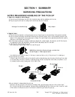
NOTES REGARDING HANDLING OF THE PICK-UP

1. Notes for transport and storage

1) The pick-up should always be left in its conductive bag until immediately prior to use.
2) The pick-up should never be subjected to external pressure or impact.

2. Repair notes

1) The pick-up incorporates a strong magnet, and so should never be brought close to magnetic materials.
2) The pick-up should always be handled correctly and carefully, taking care to avoid external pressure and

impact. If it is subjected to strong pressure or impact, the result may be an operational malfunction and/or
damage to the printed-circuit board.

3) Each and every pick-up is already individually adjusted to a high degree of precision, and for that reason

the adjustment point and installation screws should absolutely never be touched.

4) Laser beams may damage the eyes!

Absolutely never permit laser beams to enter the eyes!

Also NEVER switch ON the power to the laser output part (lens, etc.) of the pick-up if it is damaged.

5) Cleaning the lens surface

If there is dust on the lens surface, the dust should be cleaned away by using an air bush (such as used
for camera lens). The lens is held by a delicate spring. When cleaning the lens surface, therefore, a cot-
ton swab should be used, taking care not to distort this.

6) Never attempt to disassemble the pick-up.

Spring by excess pressure. If the lens is extremely dirty, apply isopropyl alcohol to the cotton swab. 
(Do not use any other liquid cleaners, because they will damage the lens.) Take care not to use too much
of this alcohol on the swab, and do not allow the alcohol to get inside the pick-up.

Storage in conductive bag

Drop impact

NEVER look directly at the laser beam, and don’t let 
contact fingers or other exposed skin.

Magnet

How to hold the pick-up

Conductive Sheet

Cotton swab

Pressure

Pressure

SECTION 1  SUMMARY

SERVICING PRECAUTIONS

Copyright © 2007 LG Electronics. Inc. All right reserved.

Only for training and service purposes

LGE Internal Use Only

Содержание FBS162V

Страница 1: ...VICE MANUAL MODEL FB162 A0U FBS162V CAUTION BEFORE SERVICING THE UNIT READ THE SERVICING PRECAUTIONS IN THIS MANUAL MINI HOME THEATER SERVICE MANUAL P NO AFN35036931 Website http biz lgservice com Internal Use Only SEPTEMBER 2007 ...

Страница 2: ...CTION 2 6 SECTION 3 INTERNAL BLOCK DIAGRAM OF IC s 3 1 SECTION 4 ELECTRICAL TROUBLESHOOTING GUIDE OF ADUIO PART 4 1 SECTION 5 ELECTRICAL TROUBLESHOOTING GUIDE OF DVD PART 5 1 SECTION 6 BLOCK DIAGRAM 6 1 SECTION 7 CIRCUIT DIAGRAM VOLTAGE CHART 7 1 SECTION 8 PRINTED CIRCUIT DIAGRAMS 8 1 SECTION 9 REPLACEMENT PARTS LIST 9 1 Copyright 2007 LG Electronics Inc All right reserved Only for training and se...

Страница 3: ...eyes Also NEVER switch ON the power to the laser output part lens etc of the pick up if it is damaged 5 Cleaning the lens surface If there is dust on the lens surface the dust should be cleaned away by using an air bush such as used for camera lens The lens is held by a delicate spring When cleaning the lens surface therefore a cot ton swab should be used taking care not to distort this 6 Never at...

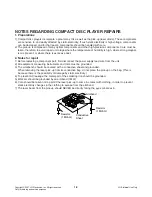
Страница 4: ...pply lead wire from the unit 2 All equipment measuring instruments and tools must be grounded 3 The workbench should be covered with a conductive sheet and grounded When removing the laser pick up from its conductive bag do not place the pick up on the bag This is because there is the possibility of damage by static electricity 4 To prevent AC leakage the metal part of the soldering iron should be...

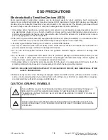
Страница 5: ... propelled chemicals These can generate electrical charges sufficient to damage ESD devices 6 Do not remove a replacement ESD device from its protective package until immediately before you are ready to install it Most replacement ESD devices are packaged with leads electrically shorted together by conductive foam aluminum foil or comparable conductive materials 7 Immediately before removing the p...

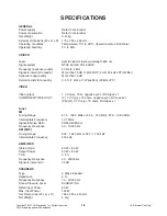
Страница 6: ...OMPONENT VIDEO OUT Y 1 0 V p p 75 ohms negative sync RCA jack x 1 Pb Pr 0 7 V p p 75 ohms RCA jack x 1 Tuner FM Tuning Range 87 5 108 0 MHz or 65 0 74 0 MHz 87 5 108 0 MHz Intermediate Frequency 10 7 MHz Signal to Noise Ratio 60 55 dB Mono Frequency Response 50 10 000 Hz AM MW Tuning Range 522 1 620 kHz or 520 1 720 kHz Intermediate Frequency 450 kHz AMPLIFIER Stereo mode 80 W 80 W Output Power 80...

Страница 7: ...Copyright 2007 LG Electronics Inc All right reserved Only for training and service purposes LGE Internal Use Only ...

Страница 8: ... 252 A26 A50 A52 A46 A44 264 468 253 257 463 300 CABLE1 CABLE2 CN303 P5701 P9701 P9702 CN302 NOTES THE EXCLAMATION POINT WITHIN AN EQUILATERAL TRIANGLE IS INTENDED TO ALERT THE SERVICE PERSONNEL TO THE PRESENCE OF IMPORTANT SAFETY INFORMATION IN SERVICE LITERATURE Copyright 2007 LG Electronics Inc All right reserved Only for training and service purposes LGE Internal Use Only A43 CABLE3 275 A47 26...

Страница 9: ...2 003 A01 020 018 014 013 017 435 012 A26 019 012 440 015B 015A 015 016 A02 439 012A 012A 010 432 030 025 024 439 431 435 430 021 036 A03 Copyright 2007 LG Electronics Inc All right reserved Only for training and service purposes LGE Internal Use Only ...
Страница 10: ...A80L 850 851 855 854 856 854 854 863 862 861 860 859 858 864 853 852 RIGHT CABINET ASS Y LEFT CABINET ASS Y RIGHT SPK ASS Y LEFT SPK ASS Y 857R 857L Copyright 2007 LG Electronics Inc All right reserved Only for training and service purposes LGE Internal Use Only ...
Страница 11: ...808 Packing 824 Antenna 825 Remote control 900 Instruction Ass y 801 Packing 803 Box 802 Bag 804 Clear Sheet 805 Accessory Bag 804A 803A Plug Ass y 1Way Red White 813 Copyright 2007 LG Electronics Inc All right reserved Only for training and service purposes LGE Internal Use Only ...
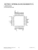
Страница 12: ...3 1 SECTION 3 INTERNAL BLOCK DIAGRAM OF IC S 1 µPD78F0546R R PIN CONFIGURATION TOP VIEW Copyright 2007 LG Electronics Inc All right reserved Only for training and service purposes LGE Internal Use Only ...
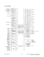
Страница 13: ...3 2 BLOCK DIAGRAM Copyright 2007 LG Electronics Inc All right reserved Only for training and service purposes LGE Internal Use Only ...

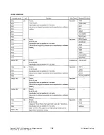
Страница 14: ...3 3 PIN FUNCTION Copyright 2007 LG Electronics Inc All right reserved Only for training and service purposes LGE Internal Use Only ...
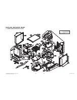
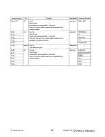
Страница 15: ...3 4 Copyright 2007 LG Electronics Inc All right reserved Only for training and service purposes LGE Internal Use Only ...
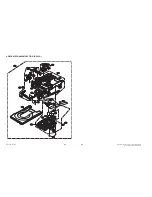
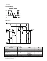
Страница 16: ...ARAMETER Supply Voltage V V 18 V Input Voltage VIC 5 V Differential Input Voltage VID 30 V Output Current Io 50 mA Power Dissipation PD 300 SOP 8 mW 800 DIP 8 250 TSSOP 8 Operating Temperature Range Topr 40 to 85 C Storage Temperature Range Tstg 40 to 125 C Copyright 2007 LG Electronics Inc All right reserved Only for training and service purposes LGE Internal Use Only ...
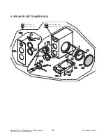
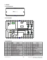
Страница 17: ...t 12 VO2 O CH2 driver output 13 VO1 O CH1 driver output 14 VO1 O CH1 driver output No SYMBOL I O SYMBOL 15 VO4 O CH4 driver output 16 VO4 O CH4 driver output 17 VO3 O CH3 driver output 18 VO3 O CH3 driver output 19 GND Ground 20 PVCC2 Power supply 2 21 MUTE I Mute 22 IN3 I CH3 input 23 IN4 I CH4 input 24 Vdet I Reset controller input 25 Reset O Reset controller output 26 REOadj O Adjustable regula...

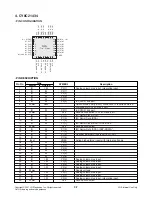
Страница 18: ... part 7 Power Vss Ground connection in CY8C21634 part 8 IO M P1 7 I2C Serial Clock SCL 9 IO M P1 5 I2C Serial Data SDA 10 IO M P1 3 11 IO M P1 1 I2C Serial Clock SCL ISSP SCLK 12 Power Vss Ground connection 13 IO M P1 0 I2C Serial Data SDA ISSP SDATA 14 IO M P1 2 15 IO M P1 4 Optional External Clock Input EXTCLK 16 IO M P1 6 17 Input XRES Active high external reset with internal pull down 18 IO M ...

Страница 19: ...2 bit storage register Q5 10 11 Q6 PIN DESCRIPTION PIN NAME FUNCTION TYPE BU2092 F BU2090 F FS BU2092 FV 1 1 1 DATA GND 2 2 2 CLOCK Serial data input 3 3 3 LCK Data shift clock input 4 4 Q0 Data latch clock input 4 5 5 Q1 Parallel data output 5 6 6 Q2 Parallel data output 6 7 7 Q3 Parallel data output 7 8 8 Q4 Parallel data output 8 9 9 Q5 Parallel data output 9 10 10 Q6 Parallel data output 10 11...

Страница 20: ...K SCLK CKS2 CKS0 SDTO BLOCK DIAGRAM Modulator MCLK AINL LRCK SCLK SDTO DIF VCOM Clock Divider AINR AGND VA Decimation Filter Serial I O Interface Voltage Reference CKS1 DGND VD CKS2 Modulator Decimation Filter PDN CKS0 Copyright 2007 LG Electronics Inc All right reserved Only for training and service purposes LGE Internal Use Only ...
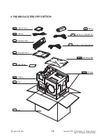
Страница 21: ...at Power down mode 10 LRCK I O Output Channel Clock Pin L Output in Master Mode at Power down mode 11 MCLK I Master Clock Input Pin 12 SCLK I O Audio Serial Data Clock Pin L Output in Master Mode at Power down mode 13 PDN I Power Down Mode Reset Pin H Power up L Power down Reset The AK5358 must be reset once upon power up 14 DIF I Audio Interface Format Pin H 24bit I2S Compatible L 24bit MSB justi...

Страница 22: ... OTW SD PWM_A RESET_AB PWM_B OC_ADJ GND AGND VREG M3 M2 M1 PWM_C RESET_CD PWM_D VDD GVDD_C GVDD_A BST_A PVDD_A OUT_A GND_A GND_B OUT_B PVDD_B BST_B BST_C PVDD_C OUT_C GND_C GND_D OUT_D PVDD_D BST_D GVDD_D DKD PACKAGE TOP VIEW Copyright 2007 LG Electronics Inc All right reserved Only for training and service purposes LGE Internal Use Only ...
Страница 23: ...M3 PVDD Power Supply Decoupling 35 V 12 V GND VAC PWM_A PWM_C PWM_D PWM_B VALID M2 Left Channel Output Right Channel Output Input H Bridge 1 Input H Bridge 2 GVDD VDD VREG Power Supply Decoupling 4 PVDD_A B C D GND_A B C D GVDD_A B C D 4 4 VDD GND VREG AGND OC_ADJ Bootstrap Capacitors 2nd Order L C Output Filter for Each Half Bridge SD OTW Output H Bridge 2 Output H Bridge 1 OTW SD TAS5508 Copyrig...

Страница 24: ...T_C Timing Gate Drive Ctrl PWM Rcv GVDD_C PWM_B OUT_B GND_B PVDD_B BST_B Timing Gate Drive Ctrl PWM Rcv GVDD_B PWM_A OUT_A GND_A PVDD_A BST_A Timing Gate Drive Ctrl PWM Rcv GVDD_A Ctrl BTL PBTLConfiguration Pulldown Resistor BTL PBTLConfiguration Pulldown Resistor BTL PBTLConfiguration Pulldown Resistor BTL PBTLConfiguration Pulldown Resistor Internal Pullup Resistors to VREG Copyright 2007 LG Ele...

Страница 25: ...1 12 13 14 15 16 1 2 3 4 5 6 7 8 30 31 32 33 34 35 36 37 26 27 28 29 76 77 78 79 80 17 18 19 20 38 39 40 41 42 43 44 45 21 22 23 24 25 IO_VDD IO_VSS IO_VDD DVDD DVSS IO_VDD IO_VDD IO_VDD DVSS DVDD IO_VDD PULSUS PS9829B BLOCK DIAGRAM PLL PWM Modulator Internal Controls MLRCK MBCK MSDIN 0 3 CLK_IN SCK SCL SO SDA SI I2C_AD0 CS I2C_AD2 PWM2_P M PWM3_P M PWM4_P M PWM5_P M PWM6_P M RESET OVERLOAD EXT_MU...

Страница 26: ...tter and soft start 3 GND Ground terminal Ground 4 FB CC OLP FB CC OLP terminal Input of constant voltage signal constant current operation control signal over load protection signal 5 Vcc Power supply terminal Input of power supply for control circuit 7 D Drain terminal MOSFET drain Input of Startup current 8 Copyright 2007 LG Electronics Inc All right reserved Only for training and service purpo...

Страница 27: ...erload Overload Protection and Soft Start peration Time set up Soft Start set up Terminal 6 FB Feedback terminal Constant Voltage Control Signal Input Burst intermittent mode Oscillation Control 7 OCP BD Overcurrent Protection Input Overcurrent Detection Signal Input Bottom Detection Terminal Bottom Detection Signal Input 10 STR X6757N Copyright 2007 LG Electronics Inc All right reserved Only for ...

Страница 28: ...nput is over 5V Check if output voltage of IC101 KIA7042 is 4 3V Check the related part of IC101 KIA7042 Replace the related parts OK Check power of both terminals of IC101 KIA7042 Check IC100 78KO KF2 1 PIN power OK YES NO NO NO NO YES YES YES YES Copyright 2007 LG Electronics Inc All right reserved Only for training and service purposes LGE Internal Use Only ...
Страница 29: ...5V Check the working condition X101 32 768kHz X100 9 8304MHz OK Check P7904 5PIN 5 6V Refer to SMPS Troubleshooting Check D101 1SR35 output is working on 5V Check the related part OK Replace the related parts Check power of both terminals of D101 1SR35 Check Q101 EMITTER 5V and COLLECTOR 5V NO NO NO NO NO YES YES YES YES YES YES YES YES YES YES YES YES Copyright 2007 LG Electronics Inc All right r...

Страница 30: ...er of each PIN OK Replace the related part OK Check P7904 1 2 3 power F1 F2 both terminals over 3 7V Check power VKK over 28V Check P7302 connection condition and power F1 F2 both terminals over 3 7V Check power VKK over 28V Check 25 PIN 5 6V Check IC301 PT6324 power 50 PIN VKK 28V 9 52 PIN 5V YES YES YES YES YES YES YES YES YES YES NO NO NO NO NO NO Copyright 2007 LG Electronics Inc All right res...

Страница 31: ...eck the related part Check 76 PIN DO DATA input Check the related part Replace the related part OK Replace the related part OK FLT light on OK IC100 75 PIN STB 78 PIN 1PIN CLK Check Data output YES YES YES YES YES YES YES YES NO NO NO NO Copyright 2007 LG Electronics Inc All right reserved Only for training and service purposes LGE Internal Use Only ...
Страница 32: ...ATA R358 OK OK OK Replace the related part IC304 29PIN check 5V Check IC304 8Pin 9Pin IC100 5Pin CLK 23Pin DATA YES YES YES NO Refer to SMPS Troubleshooting NO NO NO Copyright 2007 LG Electronics Inc All right reserved Only for training and service purposes LGE Internal Use Only ...
Страница 33: ...o SMPS Troubleshooting Check the related part of X601 OK Check R668 470Ω output OK Check resistance output of LINE DATA R671 CLK R670 RST R665 OK Check DVD ASS Y PS9829 communication condition P7403 Check IC604 PS9829 DATA input OK Check IC604 PS9829 part Replace the related part Replace the related part Replace the related part Refer to DVD Troubleshooting Check resistance output of each LINE YES...

Страница 34: ...WM MODULATOR input 4 6 14 16 PIN Check POWER IC 700 34 29 27 20 PIN output Check output LINE COIL OK Refer to SMPS Troubleshooting Check resistance power IC700 R702 701 726 727 724 Replace the related parts YES YES YES YES YES YES NO NO NO Copyright 2007 LG Electronics Inc All right reserved Only for training and service purposes LGE Internal Use Only ...
Страница 35: ...eform OK Check IC200 BU4052 16PIN VDD 8PIN VSS power Check u COM IC100 3PIN 69PIN communication Refer to SMPS Troubleshooting Replace the related parts Check IC801 MC4580 4PIN VSS 8PIN VDD power Replace the related parts YES YES YES YES YES YES NO NO NO NO Copyright 2007 LG Electronics Inc All right reserved Only for training and service purposes LGE Internal Use Only ...
Страница 36: ...the related parts Check IC801 MC4580 4PIN VSS 8PIN VDD power Check IC200 BU4052 1 12PIN input waveform Check IC200 BU4052 3 13PIN output waveform Check IC601 BU 4502 2 15PIN Check 25 PIN 5 6V Check IC801 MC4580 2 6PIN input waveform OK YES YES YES YES YES YES NO NO NO Copyright 2007 LG Electronics Inc All right reserved Only for training and service purposes LGE Internal Use Only ...
Страница 37: ...k the DC V Of C909 C903 C921 If DC V is in 14 19V and it is steady Replace the fuse Check BD901 LF901 902 Check IC901 902 Replace IC 901 902 Check short of P9702 line Check short of P9701 line Check short of P9701 P9702 line MAIN PART YES NO YES YES YES YES YES NO NO NO NO NO Copyright 2007 LG Electronics Inc All right reserved Only for training and service purposes LGE Internal Use Only ...

Страница 38: ...er circuit Trouble shooting P SENS PART Check the PIN3 OF P9702 If DC V is over 30V 1 OK Check power circuit Trouble shooting VKK PART YES YES NO NO Copyright 2007 LG Electronics Inc All right reserved Only for training and service purposes LGE Internal Use Only ...

Страница 39: ...pin 30pin Check the P5801 13pin and 30pin line OK YES YES YES YES NO OSD IPOD OK Check the P5801 18pin 19pin Check the P5801 18pin and 19pin line OK YES YES YES NO Copyright 2007 LG Electronics Inc All right reserved Only for training and service purposes LGE Internal Use Only ...

Страница 40: ...ule Check connector P7501 Reconnect it Does it appear DVD ERROR at FLD Select the DVD Mode Check Connector P4405 P4407 P4408 Check an Audio Micom or interface reconnect P4703 OK Does No DISC or Time are appeared at FLD NO NO NO NO YES YES YES YES YES YES Copyright 2007 LG Electronics Inc All right reserved Only for training and service purposes LGE Internal Use Only ...

Страница 41: ...F ES8380 TO IC401 FOR CONTROL OPEN CLOSE Check the Tray control I O Pin on IC401 OPEN CLOSE signals on IC401 are OK Load load signals on P401 are OK Check the cable connection between DVD PCB and MD MECHA Does tray move inside when it is at closed position ES8380 VIDEO outputs properly Check connection lines between FLASH E8380 or the FLASH access time whether is suitable or not YES YES YES YES YE...

Страница 42: ...tor driver IC401 Check Focus connection on ES8380 and motor driver IC Check the related circuit of SLED and Motor driver IC IC401 Check the MD Check cable connection with pick up head Do not put in disc and tray close Optical Lens is moving for searching Focus B C YES YES YES YES YES YES YES NO NO NO NO NO NO Copyright 2007 LG Electronics Inc All right reserved Only for training and service purpos...

Страница 43: ...control of motor driver IC404 Check the SPINDLE related circuit on ES8380 Check the related circuit of laser power transistor Check the laser power circuit between ES8380 and power transistor Q405 Q406 Collector voltage of power transistor is ok Q405 Q406 Put disc in tray Does SPINDLE rotate D YES YES YES YES YES YES YES NO NO NO NO NO NO NO Copyright 2007 LG Electronics Inc All right reserved Onl...

Страница 44: ...eck the Tracking control on motor driver IC401 Proper FOO signal on IC401 Check cable connection between P400 and MD Proper TRO signal on IC401 T T output properly Check cable connection on pick up head Check RF signal waveform Track On OK Disc play YES YES YES YES YES YES NO NO NO NO NO NO NO Copyright 2007 LG Electronics Inc All right reserved Only for training and service purposes LGE Internal ...

Страница 45: ...l data on ES8380 is OK For example composite video Check the video mute TR Q411 Output of Video buffer IC IC407 and ES8380 video signal data Check the connections between ES8380 and P4703 NO NO NO NO YES YES Copyright 2007 LG Electronics Inc All right reserved Only for training and service purposes LGE Internal Use Only ...

Страница 46: ...RST signal Check the USB PART and DVD PART line Check the USB JACK POWER supply Check P5301 Check the USB DATA LINE P5301 Check the IC501 ES8380 Check DATA LINE PIN 97 USB No 98 USB Po NO NO YES YES YES YES YES YES YES Copyright 2007 LG Electronics Inc All right reserved Only for training and service purposes LGE Internal Use Only ...

Страница 47: ...ET DATA ETC WAVEFORM 1 RESET DVD 2 RX 3 TX 4 LCS3 FLASH Playing at USB function 1 HRST 2 5V 3 D 4 D 4 WAVEFORMS Copyright 2007 LG Electronics Inc All right reserved Only for training and service purposes LGE Internal Use Only ...

Страница 48: ...POWER ON 3 STARTING ACTION WAVEFORM IN MD DEVICE 1 Limit SW 2 OPEN 3 CLOSE 1 SLO from MPEG 2 SLED 3 SLED At Power on Copyright 2007 LG Electronics Inc All right reserved Only for training and service purposes LGE Internal Use Only ...

Страница 49: ...5 10 4 FOCUS WAVEFORM 1 FDO 2 F 3 F INSERT CD INSERT DVD 1 FDO 2 F 3 F Copyright 2007 LG Electronics Inc All right reserved Only for training and service purposes LGE Internal Use Only ...

Страница 50: ...in 3 Spin 1 A 2 B 3 C 4 D 5 AT POWER ON SPINDLE SIGNAL AT MD DECK 6 AT FIRST ACTION FOCUS SIGNAL A B C D Copyright 2007 LG Electronics Inc All right reserved Only for training and service purposes LGE Internal Use Only ...

Страница 51: ...5 12 7 TRACKING SIGNAL 8 RF WAVEFORM 1 Tro 2 Tr 3 Tr Copyright 2007 LG Electronics Inc All right reserved Only for training and service purposes LGE Internal Use Only ...

Страница 52: ...5 13 9 DISK TYPE JUGEMENT WAVEFORM 1 F 2 FDO 3 SVRRF DVD CD Copyright 2007 LG Electronics Inc All right reserved Only for training and service purposes LGE Internal Use Only ...

Страница 53: ...Copyright 2007 LG Electronics Inc All right reserved Only for training and service purposes LGE Internal Use Only ...

Страница 54: ...N 6 BLOCK DIAGRAM 1 WIRING DIAGRAM A 1 2 3 4 5 6 7 8 9 10 11 12 B C D E F G H I J K L M N O P Q R S T Copyright 2007 LG Electronics Inc All right reserved Only for training and service purposes LGE Internal Use Only ...

Страница 55: ... 2 MAIN TOTAL BLOCK DIAGRAM A 1 2 3 4 5 6 7 8 9 10 11 12 B C D E F G H I J K L M N O P Q R S T Copyright 2007 LG Electronics Inc All right reserved Only for training and service purposes LGE Internal Use Only ...

Страница 56: ...FL1 FL2 4 5V 12V 12V 78R12 5V P SENS FEED BACK 6 1V KIA278R05 P9702 P9701 FEED BACK AMP 29V 3 5V 278R35 31 5V VKK A 1 2 3 4 5 6 7 8 9 10 11 12 B C D E F G H I J K L M N O P Q R S T 3 SMPS BLOCK DIAGRAM Copyright 2007 LG Electronics Inc All right reserved Only for training and service purposes LGE Internal Use Only ...

Страница 57: ... 6 8 4 DVD BLOCK DIAGRAM A 1 2 3 4 5 6 7 8 9 10 11 12 B C D E F G H I J K L M N O P Q R S T Copyright 2007 LG Electronics Inc All right reserved Only for training and service purposes LGE Internal Use Only ...

Страница 58: ... SCHEMATIC FOR EASY IDENTIFICATION THIS CIRCUIT DIAGRAM MAY OCCASIONALLY DIFFER FROM THE ACTU AL CIRCUIT USED THIS WAY IMPLEMENTATION OF THE LATEST SAFETY AND PERFORMANCE IMPROVEMENT CHANGES INTO THE SET IS NOT DELAYED UNTIL THE NEW SERVICE LIT ERATURE IS PRINTED 1 Shaded parts are critical for safety Replace only with specified part number 2 Voltages are DC measured with a digital volt meter duri...

Страница 59: ...7 3 7 4 2 MAIN CIRCUIT DIAGRAM Copyright 2007 LG Electronics Inc All right reserved Only for training and service purposes LGE Internal Use Only ...

Страница 60: ...7 5 7 6 3 FRONT CIRCUIT DIAGRAM Copyright 2007 LG Electronics Inc All right reserved Only for training and service purposes LGE Internal Use Only ...

Страница 61: ...7 7 7 8 4 MAIN AMP CIRCUIT DIAGRAM Copyright 2007 LG Electronics Inc All right reserved Only for training and service purposes LGE Internal Use Only ...

Страница 62: ...7 9 7 10 5 MPEG CIRCUIT DIAGRAM Copyright 2007 LG Electronics Inc All right reserved Only for training and service purposes LGE Internal Use Only ...

Страница 63: ...7 11 7 12 6 SERVO CIRCUIT DIAGRAM Copyright 2007 LG Electronics Inc All right reserved Only for training and service purposes LGE Internal Use Only ...

Страница 64: ...7 13 7 14 7 INTERFACE CIRCUIT DIAGRAM Copyright 2007 LG Electronics Inc All right reserved Only for training and service purposes LGE Internal Use Only ...

Страница 65: ...7 15 7 16 8 TOUCH PAD1 KEY CIRCUIT DIAGRAM Copyright 2007 LG Electronics Inc All right reserved Only for training and service purposes LGE Internal Use Only ...

Страница 66: ...7 17 7 18 9 TOUCH PAD2 VOLUME CIRCUIT DIAGRAM Copyright 2007 LG Electronics Inc All right reserved Only for training and service purposes LGE Internal Use Only ...

Страница 67: ...0PIN 3 43V 13PIN 1 9V 22PIN 3 43V 29PIN 3 43V 34PIN 1 9V 39PIN 3 43V 42PIN 1 9V 47PIN 3 43V 56PIN 3 43V 65PIN 3 44V 66PIN 1 9V 72PIN 3 44V 80PIN 1 9V 87PIN 3 4V 91PIN 1 9V 94PIN 3 4V IC605 8PIN 3 4V IC700 17PIN 11 8V 21PIN 29V 26PIN 29V 29PIN 29V 34PIN 29V IC801 8PIN 11 6V IC100 19PIN 4 87V 20PIN 4 87V 59PIN 4 87V IC103 8PIN 4 87V IC301 9PIN 4 8V 51PIN 4 8V IC302 6PIN 10 8V IC303 15PIN 5 22V IC304...

Страница 68: ...8 1 8 2 SECTION 8 PRINTED CIRCUIT DIAGRAMS 1 MAIN P C BOARD TOP SIDE Copyright 2007 LG Electronics Inc All right reserved Only for training and service purposes LGE Internal Use Only ...

Страница 69: ...8 3 8 4 2 MAIN P C BOARD BOTTOM SIDE Copyright 2007 LG Electronics Inc All right reserved Only for training and service purposes LGE Internal Use Only ...

Страница 70: ...8 5 8 6 3 DVD P C BOARD TOP SIDE BOTTOM SIDE Copyright 2007 LG Electronics Inc All right reserved Only for training and service purposes LGE Internal Use Only ...

Страница 71: ...8 7 8 8 4 FRONT P C BOARD Copyright 2007 LG Electronics Inc All right reserved Only for training and service purposes LGE Internal Use Only ...

Страница 72: ...C BOARD NOTES Warning Parts that are shaded are critical with respect to risk of fire or electricial shock Copyright 2007 LG Electronics Inc All right reserved Only for training and service purposes LGE Internal Use Only ...

Страница 73: ...8 11 8 12 6 TOUCH PAD P C BOARD Copyright 2007 LG Electronics Inc All right reserved Only for training and service purposes LGE Internal Use Only ...

Отзывы: