background image

52

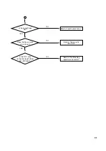
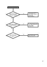
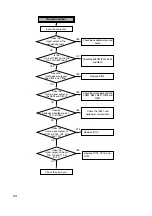
Check the cold soldering for

the IC501(BA5983FM)

pin 13, 14.

Replace IC501. 

Check the FG1 signal line.

Check the cold soldering for

the IC401.

YES

NO

YES

A

B

NO

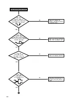
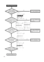
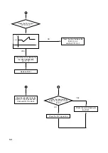
Check the circuit between the

IC401 Pin 3, 4

and the IC701 Pin 4.

C

Check the FAO signal.

(IC701 Pin 4 )

Does the square wave 

output at the IC401 Pin 24

(FG1)?

V

1.35V

T

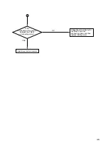
Check the cold soldering  for the

IC301 Pin 1, 38, 40, 63 and C301,

C303 and IC701 Pin 38, 34.

Содержание DRD-8080B

Страница 1: ... Random Access Time CD Supports 8X max Rotational Modes in DVD Mode Supports 40X max Rotational Modes in CD Mode Max 10 800 kB sec Sustained Transfer rate in DVD mode Max 6 000 kB sec Sustained Transfer rate in CD mode Photo CD Multisession Disc Spec compliant Multimedia MPC 3 Spec compliant Power Tray Loading Ejection Mechanism 3 Way Eject Support Software Open Close Button Emergency Eject Closed...

Страница 2: ...omputer to this connector COMPACT COMPACT 1 2 4 3 R O M R O M R O M R O M 5 6 DIGITAL ANALOG INTERFACE POWER D R C S M S L A G L G 39 1 5 12 GND 40 2 AUDIO AUDIO 1 2 5 4 3 FRONT VIEW BACK VIEW 1 Headphone Jack Standard 1 8 3 5mm stereo jack for listening to the audio signal from audio CDs 2 Headphone Volume Control Adjusts the headphone sound level 3 Disc Drawer Accepts a CD ROM DVD ROM disc on it...

Страница 3: ...et in the direction of arrow 4 See Fig 1 3 B Remove the CD Tray drawing forward by pushing the Hook a backward 5 C Remove the Main Circuit Board in the direction of arrow 6 D At this time be careful not to damage the 4 connectors are positioned at side of the Main Circuit Board 2 DECK ASSY DISASSEMBLY 2 1 Base Assy A Release 1 screw C and 2 Stoppers D B Separate the Base Assy in the direction of a...

Страница 4: ...pring B Remove the Pick up Unit 2 3 Feeding Motor Assy A Remove the Feeding Motor Assy by pushing the 2 hooks b B At this time be careful the hooks of the Base Pick up Skew Spring Pick up Unit Fig 1 5 Base Pick up Feeding Motor Assy Fig 1 6 ...

Страница 5: ...1 DVD C CN12 DVD D CN7 DVD RF CN13 DVD E CN5 DVD F CN19 DVD VR CN18 DVD MD CN16 DVD LD CN15 DVD LD GND CN1 FO CN2 FO CN3 TR CN4 TR CN30 CD VCC CN20 CD VC CN26 CD GND CN25 CD A CN28 CD B CN23 CD C CN24 CD E CN29 CD F CN21 CD VR CN22 CD MD CN27 CD LD C010 C011 C012 VR02 U002 U001 TRACKING FOCUS C004 ACTUATOR VR01 LASER DIODE LASER DIODE PICK UNIT ...

Страница 6: ...thod F E In case of CD Disc This signal is generated in RF AMP IC IC301 SSI3723 and controls the pick up s left and right shift to find the track on CD Disc 3 RF Signal A B 2C In case of CD Disc This signal is converted to DATA signal in DSP IC IC701 CXD3030R 2 Structure of the Photo Diode CD Infrared laser Pick Up module Photo Diode Tracking Focusing As seen from light receiving side E C B F A ...

Страница 7: ... phase of A C and B D In case of DVD Disc This signal is generated in RF AMP IC IC301 SSI3723 and controls the pick up s left and right shift to find the track on DVD Disc 3 RF Signal A B C D In case of DVD Disc This signal is converted to DATA signal in DSP IC IC201 CXD1867R 3 Structure of the Photo Diode DVD As seen from light receiving side Red laser Pick Up module Photo Diode Tracking Focusing...

Страница 8: ...ent Driver Control output of the LD Laser Diode The detect current from the monitor diode converts to the I V Current Voltage at the external resistor Beforehand it adjusts a fixed level over for a standard GND If this voltage inputs to the PD IN IC301 Pin 23 24 it is amplified about 36 4 times about 31 2dB So this voltage outputs from the LD OUT IC301 Pin 21 22 The LD driving element Q302 Q303 us...

Страница 9: ...13 14 15 16 AMP AMP MUX ATT AGC AGC 40 GCA GCA SUM AMP BUFF MUX MUX FE TE RF AC To IC701 38 To IC701 36 To IC701 47 To IC202 117 GCA 39 57 EQ Phase Detector EQ DVD A B C D DVD A2 B2 C2 D2 CD E F Pick up Unit PN301 IC301 SSI3723 4 4 RF DC RF SIN 63 2 RF Amplifier Circuit 2 1 RF AMP Constitution ...

Страница 10: ...ACKING ACTUATOR IC501 DRIVE BA5983FM IC701 CD DVD SERVO DSP CXD3030R F F T T LEVEL SHIFT LEVEL SHIFT FAO TAO D A DIGITAL EQUALIZER AUTO ADJUSTMENT CIRCUIT SLED Control Signal A D TE FE TE SAO SLED MOTOR Hall Sensor M PHO C PHO A FEED MOTOR FEED MOTOR LEVEL SHIFT IC501 Q501 DRIVE BA5983FM KTD1304 IC201 u COM SLGNCHG SLED CLK A B C A B C D A2 B2 C2 D2 3 Focus Tracking Sled Servo Circuit 3 1 FOCUS TR...

Страница 11: ... differs from each other and the generated signal output through the TE terminal This signal input to TE of IC701 after the first amplification and converted to A D The signal converted to A D input to the Digital Equalizer assigned the most important part at the Tracking Servo Tracking Servo Gain is generated with Digital Filter coefficient value set according to the disc at the µ COM Tracking si...

Страница 12: ... SPDG1 2 4 Spindle Servo Circuit 4 1 SPINDLE SERVO PROCESS 4 2 Spindle Servo for CD DVD DRD 8080B consists of the three spindle control respectively 1 DVD x 8 CAV DVD Single Dual Layer 2 CD x 16 max CAV CD DA CD RW 8 20 x Video CD 8x CLV Host command stand by of CD ROM and CD R 3 CD x 40 max CAV CD R CD ROM play mode In the spindle speed control mode respectively CD x 16 Max CD x 40 Max CAV drives...

Страница 13: ...ing IC CD TE FE SLED Spindle Control Command Data Status SDATA CD DATA CD RF MA 0 8 MDB 0 F DATA 0 7 ADR 0 8 SICLK SIXLT SIDAT SCLK CD Data ECC Receive the order from Host 2 nd ECC CD Data Buffering Generating RF Signal Generating Tracking Error Generating Focusing Error CD Servo Control CD Data Flow Control Host Command Receive or Data Status Transfer Error Correction Generating Header Sync Gener...

Страница 14: ... MA 0 8 MDB 0 F Generating A B E F Signal SSI3723 RF Signal processing IC Generating RF Signal Generating Tracking Error Generating Focusing Error Error Signal Receive the Command from Host DVD Data Buffering Copy Protection Control DVD Data Buffering DVD Servo Control DVD Data Flow Control Host Command Receive or Data Status transfer EDC ECC processing Generating DVD ID Sync EFM Demodulation ...

Страница 15: ...ads the regional code and plays title in the case of allowed regional code only 2 Management of DVD Disc for the scrambled of data 1 DVD ROM and DVD player of host generate the KEY 1 respectively transfer to opposite part the KEY 2 is received recognizes the data transfer or not with this value and generates the bus key encoded the data 2 Encoded Disc Key and Title Key host is transfer with the bu...

Страница 16: ...MPEG 2 board generates the challenge key 10 Byte and transfers to drive The board and drive generate key 1 5Byte with the challenge key respectively Of course the Algorithm generating the key 1 is not known 3 Compare with the generated key 1 if it corresponds each other the first step of authentication is completed This is a course to identify the MPEG 2 board with a drive 4 The second step of aut...

Страница 17: ...UM PLW PNG NZL AUS 4 The disc has the regional code of 8 bit Example The disc manufactured in the U S A has the number one Transfer to MPEG 2 board reading the regional code Receiving data from the MPEG 2 board and output through the monitor If the board is setting to the regional code 1 for the U S A Check the received regional code to number 1 all or not transfer the data to VGA card in accordan...

Страница 18: ...p Clamp Env Inv 10 PIOR b4 0 70kHz 15 CCR b4 0 6dB 4bit 6dB 4bit 6 FOCR b3 0 PII 14 CBR b1 0 14 CBR b3 2 SEL Buff 5 4 9 CTCR b3 0 6dB normal COMP 9 CTCR b7 BCA DET SEL PI FE TE CE V25 V125 V25 3 MNTR Control 10 PIOR b7 5 14 CBR b5 4 16 CDR b5 HLDEN 18 CFR b2 0 CE ATT 18 CFR b3 CEPOL 5 RFCR b2 0 EQ EQ EQ EQ 3 3 Comp PHASE DETECTOR PHASE DETECTOR LPF MUX SUB OFFSET Cancel GCA TE RST 1 PDCR b3 CD DVD...

Страница 19: ...and full wave rectifier PHOTO DETECTOR INTERFACE INPUTS Inputs from the main beam Photo detector matrix outputs PHOTO DETECTOR INTERFACE INPUTS AC coupled inputs for the DPD from the main beam Photo detector matrix outputs CD PHOTO DETECTOR INTERFACE INPUTS CD_A B C D come from the CD main beam Photo detector matrix outputs CD PHOTO DETECTOR INTERFACE INPUTS CD side beam photo dector outputs and u...

Страница 20: ...d by PIOR bit7 5 Pin No 61 62 52 53 57 64 40 39 41 32 34 27 38 21 22 42 Type O O O O O O O O O O O O O O OUTPUT PINS Name BYP CP CN LCP LCN MP MB MEV MLPF TPH VC V125 RX Description The RF AGC integration capacitor CBYP is connected between BYP and VPA DIFFERENTIAL PHASE TRACKING LPF PIN The external capacitance is connected between CN DIFFERENTIAL PHASE TRACKING LPF PIN The external capacitance i...

Страница 21: ... left open SERIAL DATA Serial data bidirectional CMOS pin V33 NRZ programming data for the internal registers is applied to this input not to be left open SERIAL CLOCK Serial clock CMOS input The clock applied to this pin is synchronized with the data applied to SDATA not to be left open Pin No 48 47 46 Type I I O I SERIAL PORT PINS ...

Страница 22: ... BA5983 Serial data latch output Sub Q serial clock to CXD3030R Serial clock signal to CXD3030R SENS serial clock to CXD3030R Offset input for Focus actuator to Q503 base Offset input for Focus actuator to Q504 base Spindle Gain control signal 0 Spindle Gain control signal 1 GND Short brake output signal to spindle driver IC 401 Audio Mute Control RF signal Pass change Flash memory writing enable ...

Страница 23: ...Tray closed S W input NC P up limit S W input NC NC GND Wait signal to CXD1867R SP3723 enable data SP3723 control data NC Hardware standby mode transition input Reset input from reset part NC GND 16MHz external clock input NC 5V NC Read signal to CXD1867R Write signal to CXD1867R NC Operating mode control 0 Operating mode control 1 Operating mode control 2 5V Referance voltage for A D D A converte...

Страница 24: ...t from CXD1867R Int1 request from CXD1867R FOK input signal from CXD3030R Sub code sync input signal from CXD1867R CXD303 NC GND COUT from CXD3030R CD DVD spindle signal pass change Sled motor rotation senser clock input Spindle motor rotation sensor clock input Spindle motor rotation sensor clock input MIRR input from SP3723 BCARF input from SP3723 Actuator driver ic mute control H8 3062 pin name...

Страница 25: ...CC FDO LPF1 LPF2 VC1 LPF5 VCOR1 VCOIN MDPOUT MDSOUT CLVS MDIN1 MDIN2 SPO VC2 GFS APEO GSCOR MDAT BCLK LRCK C2PO WFCK SCOR SBIN EXCK XRCI DDAT DLRC DBCK XTAL XWR XRD D 7 0 A 7 0 XCS XINT0 XINT1 XWAIT 79 80 82 87 89 66 69 71 73 75 96 97 99 101 102 104 106 24 26 27 29 32 34 35 37 39 41 43 45 HDB F 0 56 59 60 1 2 4 172 176 5 7 9 14 RF Asymmetry DMA Controller Priority resolve Sequencer DVD Main Data E...

Страница 26: ...3 3 8mA 8mA 5V tolerant 22 VDD 3 3 23 XHRS I 5 0 ATAPI PULL UP 24 HDB7 I O 5 0 4mA 12mA ATAPI 25 Vss DGND 26 HDB8 I O 5 0 4mA 12mA ATAPI 27 HDB6 I O 5 0 4mA 12mA ATAPI 28 VDDS 5 0 29 HDB9 I O 5 0 4mA 12mA ATAPI 30 HDB5 I O 5 0 4mA 12mA ATAPI 31 HDBA I O 5 0 4mA 12mA ATAPI 32 HDB4 I O 5 0 4mA 12mA ATAPI 33 Vss DGND 34 HDBB I O 5 0 4mA 12mA ATAPI 35 HDB3 I O 5 0 4mA 12mA ATAPI 36 VDD 3 3 37 HDBC I O...

Страница 27: ... 3 4mA 4mA 5V tolerant 72 VDD5V 5 0 73 MDB5 I O 3 3 4mA 4mA 5V tolerant 74 MDB6 I O 3 3 4mA 4mA 5V tolerant 75 MDB7 I O 3 3 4mA 4mA 5V tolerant 76 XMWR I O 3 3 4mA 4mA 5V tolerant 77 VDD 3 3 78 XRAS I O 3 3 4mA 4mA 5V tolerant 79 MA0 O 3 3 4mA 4mA 80 MA1 O 3 3 4mA 4mA 81 Vss DGND 82 MA2 O 3 3 4mA 4mA 83 MA3 O 3 3 4mA 4mA 84 MA4 O 3 3 4mA 4mA 85 MA5 O 3 3 4mA 4mA 86 MA6 O 3 3 4mA 4mA 87 MA7 O 3 3 4...

Страница 28: ...4 AGND 123 GNDA3 AGND 124 LPF5 3 3 125 VC1 3 3 126 LPF2 3 3 127 LPF1 3 3 128 VccA3 3 3 129 VccA2 3 3 130 PDO 3 3 131 PDHVCC 3 3 132 FDO 3 3 133 GNDA2 AGND 134 GNDA1 AGND 135 SPO 3 3 136 VC2 3 3 137 MDIN2 3 3 138 MDIN1 3 3 139 VccA1 3 3 140 CLVS I O 3 3 4mA 4mA 5V tolerant 141 Vss DGND 142 MDSOUT I O 3 3 4mA 4mA 5V tolerant 143 VDD 3 3 144 MDPOUT I O 3 3 4mA 4mA 5V tolerant 145 DFCT LINK I O 5 0 4m...

Страница 29: ...0 4mA 4mA 160 MDAT I O 5 0 4mA 4mA 5V tolerant Hystelesis type 161 Vss DGND 162 DLRC O 5 0 4mA 4mA 163 LRCK I 5 0 5V tolerant Hystelesis type 164 XRST I 5 0 Hystelesis type 165 IFS0 I 3 3 166 IFS1 I 3 3 167 XTAL I 5 0 168 Vss DGND 169 XTL2 O 3 3 170 XTL1 I 3 3 171 VDD 3 3 172 D0 I O 3 3 4mA 4mA 5V tolerant 173 D1 I O 3 3 4mA 4mA 5V tolerant 174 D2 I O 3 3 4mA 4mA 5V tolerant 175 D3 I O 3 3 4mA 4mA...

Страница 30: ...tor N C Output2 for motor N C N C Output1 for motor GND Hall input Amp1 positive input Hall input Amp1 negative input Hall input Amp2 positive input Hall input Amp2 negative input Hall input Amp3 positive input Hall input Amp3 negative input Hall Bias Change for BRAKE MODE Capacitor connection pin for phase compensation Short brake terminal 3 phase synthesized FG signal output terminal Rotation de...

Страница 31: ...output Driver CH4 negative output Driver CH1 positive output Driver CH4 positive output Driver CH3 negative output Driver CH3 positive output Driver CH1 output Driver CH2 output OPIN1 OPIN2 OPIN3 OPIN1 OPIN2 OPIN3 OPIN4 PreVcc PreVcc OPIN4 OPOUT 1 OPOUT 2 CH3 output OPOUT 3 OPOUT 4 8 9 10 11 12 13 14 GND GND CH1 3 standby control STBY1 PowVcc1 PowVcc CH1 2 PowVcc2 STBY2 GND GND PowVcc CH3 4 CH4 st...

Страница 32: ...erface Servo Interface SERVO DSP DAC OpAmp FOCUS SERVO TRACKINGSERVO FOCUS SLED TRACKING SLED SERVO OpAmp AnaSw A D CONVERTER MIRR DFCT FOK Peak detector Error corrector data processor Serial parallel processor Register XTLO BSSD XTLI VPCO1 XTSL PCMDI BCKI LRCKI DTSO XWO RMUTO LMUTO Error Rate Counter sequencer OSC MCKO V16M VCKI FSTIO C4M C16M VCTL PCO VCOI FILI FILO CLTV RFAC ASYI ASYO ASYE WFCK...

Страница 33: ...nput of spindle motor 14 DFCT I O 1 0 Defect signal input output 15 ATSK I Pin for Anti shock 16 MNT0 O 1 0 MNT0 output signal 17 MNT1 O 1 0 MNT1 output signal 18 MNT2 O 1 0 MNT2 output signal 19 MNT3 O 1 0 MNT3 output signal 20 VDC0 Digital power supply 2 5V 21 XRST I System reset L for resetting 22 VSC0 Digital GND 23 MTST0 I Normally H 24 MTST1 I Normally L 25 XPLCK O 1 0 XPLCK Signal output 26...

Страница 34: ...ital GND 55 VSC2 Digital GND 56 FOK I O 1 0 Focus OK input output 57 MIRR I O 1 0 Mirror signal input output 58 COUT I O 1 0 Track number count signal input output 59 GFS O 1 0 GFS output 60 SCOR O 1 0 H when subcode sync S0 or S1 is detected 61 SQSO O 1 0 Outputs 80bit Sub Q and 16 bit PCM peak level data 62 SQCK I Clock input for reading SQSO 63 SENS O 1 Z 0 SENS output Sub CPU output 64 SCLK I ...

Страница 35: ... 0 D A interface for 48 bit slot Word clock f 2Fs 91 SBSO O 1 0 Serial output of Sub P to W 92 VDIO2 Digital power supply 3 3V 93 MON O Normally open 94 V16M O 1 0 Output of VCO2 oscillation for vari pitch EFM PLL 95 TEST I Test pin Normally L 96 DTS0 I Test pin Normally L 97 DATA I Serial Data input from CPU 98 CLCK I Serial Data transfer clock input from CPU 99 XLAT I Latch input from CPU 100 FS...

Страница 36: ... D A interface for 48 bit slot serial data 117 HDBC O Normally open 118 BCK48 O 1 0 D A interface for 48 bit slot bit clock 119 VDIO3 Digital power supply 3 8V 120 HDBB O Normally open 121 GTOP O 1 0 GTOP output 122 HDBA O Normally open 123 XUGF O 1 0 XUGF output 124 VSIO4 Digital power supply GND 125 HDB9 O Normally open 126 C2PO O 1 0 C2PO output 127 HDB8 O Normally open 128 XRAOF O 1 0 XRAOF ou...

Страница 37: ... pin 3 of IC103 2 7V Check the VREF line NO Is the pin 36 of IC301 1 35V Replace IC101 3 3V Regulator NO YES YES OK Is the pin 3 of IC101 3 3V Replace X201 and X701 when the power supply of IC201 and IC701 is OK NO YES Do the X201 and X701 oscillating Replace IC203 when the IC101 3 3V Regulator Reset IC is non ok NO YES Does the pin 63 of IC203 change 0V to 5V at the power supply initial input mod...

Страница 38: ... Diode is not on A NO Refer to Servo part is abnormal NO YES Is the Laser Diode ON Does the Focus move up and down Refer to Disc Reading operation is abnormal NO YES Is the TOC area on the disc read Does the LED flicker ...

Страница 39: ...he R504 R524 R511 or pattern short NO Does the waveform appear at the R524 connected to IC501 pin 26 that is connected to IC501 reversely close normal open Does the signal appear at the IC501 pin 15 and 16 closing period Pin 15 Pin 16 opening period YES Check and replace the IC203 NO Does the IC203 pin 13 and 85 appear in the tray open close mode YES YES Check the cold soldering for the IC501 and ...

Страница 40: ...45 B Is the connecting status normal between the PN502 and loading motor Check the cold soldering for the PN502 and wire connecting status and then replace loading motor NO YES Open close mode is normal ...

Страница 41: ...eck the cold soldering for the transistor Q302 and then replace Q302 Replace the Pick up YES YES NO NO NO NO CD PART DVD PART NO Does the focusing actuator move up and down Is the PN301 pin 16 about 2V at the initial power on mode Does the signal appear at IC301 Pin 21 Is the collector of transistor Q302 about 2V YES YES Does the signal appear at IC301 Pin 26 C 3V 5V 0V 5V LD ON OK ...

Страница 42: ... for the transistor Q301 and then replace Q301 Does the signal appear at IC301 Pin 22 Is the collector of transistor Q301 about 2V 3V 5V Check the cold soldering for the IC301 and then replace IC301 Check the cold soldering for the IC203 and then replace IC203 NO YES Does the signal appear at IC301 Pin 26 YES OK 0V 5V LD ON ...

Страница 43: ... up Check the CD RF SIGNAL NO YES Does the RF out signal output IC301 pin 64 CD RF Check the cold soldering for the C329 C330 Replace IC301 NO YES Does the RF signal output at the IC301 Pin 57 RF Level about 1 2V Check the cold soldering for the C712 C713 and Q701 NO Does the RF signal input to the IC701 Pin 47 ...

Страница 44: ...O YES Does the RF out signal output from the pick up IC301 pin 1 DVD RF Check the cold soldering for the C301 C309 C304 C305 C306 C307 and C308 Replace IC301 NO YES Does the RF signal output from the IC301 pin57 RF Level about 1 2V Check the cold soldering for the R264 C220 and IC201 NO Does the RF signal output from the IC201 pin117 ...

Страница 45: ...402 normally CD IC402 pin7 Fig 2 DVD IC402 pin6 Fig 3 Fig 2 Check the cold soldering for the R414 R406 R407 R404 R405 and IC503 and then replace IC503 NO YES Does the IC401 spindle driving signal output from pin22 normally Fig 4 For CD and DVD Fig 4 Check the cold soldering for the IC401 and then replace IC401 Replace the Spindle motor NO YES YES Does the spindle driving signal output from IC401 p...

Страница 46: ...o Laser Diode is not ON YES YES YES YES YES YES YES YES NO NO Check the cold soldering for the IC701 and IC202 A B NO NO NO NO NO C CD CGFS IC701 Pin 59 DVD DGFS IC202 Pin 107 Does the pick up slide inner track Does the disc rotate Is the Laser Diode on Does the focus move up and down Is the FOK signal H IC701 Pin 56 Does the disc rotate in high speed repeatedly Is the GFS signal H OK ...

Страница 47: ...heck the cold soldering for the IC401 YES NO YES A B NO Check the circuit between the IC401 Pin 3 4 and the IC701 Pin 4 C Check the FAO signal IC701 Pin 4 Does the square wave output at the IC401 Pin 24 FG1 V 1 35V T Check the cold soldering for the IC301 Pin 1 38 40 63 and C301 C303 and IC701 Pin 38 34 ...

Страница 48: ...n 12 Check the cold soldering for the IC701 CXD3030 Check the X tal oscillating 33 8688MHz at the IC701 CXD3030 Pin 138 and 139 Check the IC701 CXD3030 Pin 97 98 and 99 µ com I F line Check the cold soldering for the IC201 H8 3062 µ com Check the cold soldering for the IC401 BA6664 NO YES YES YES NO Does the above signal output after the tray close Does the above signal output after the tray close...

Страница 49: ...al components NO NO Replace IC701 Replace R718 R719 and R720 NO Check the servo part Does the signal output at the headphone jack Is the pin 4 of IC801 and is the Pin 2 of IC802 is 5V Does the Audio signal output at the C815 and C816 Does the Audio signal output at the C804 and C805 Does the Audio signal inputted at pin 6 7 10 11 of IC801 Does the Audio signal output at IC701 pin 134 135 142 and 1...

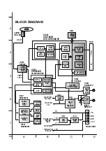
Страница 50: ...Authentication A V Dec I F DMA I F ATAPI I F DRAM 512kB Sync Det CLV Servo Sync det Loading Sled Motor Drive Loading Motor Sled Motor Tracking Focus Tracking Focus coil Head phone Amp Audio Line Amp Reset Regulator SYSTEM CONTROLLER RN5RZ 27BA NJM 3414 NJM 2100 CD SERVO DSP LASER PICK UP IC301 SP3723 IC202 H O S T I F A B C D 1 2 3 4 5 CD DVD RF AMP EQ IC502 IC103 IC204 To Motor Drive IC401 501 To...

Страница 51: ...C B A A B C D E F G H 1 2 3 4 5 002 003 007 023 017 017 024 025 413 413 413 413 430 018 022 443 011 015 420 009 427 010 014 012 008 006 005 004 027 021 019 400 013 020 001 016 026 A02 A03 A01 434 7 8 EXPLODED VIEW ...

Отзывы: