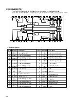
Name
VPA
VPB
VNA
VNB
V33
V25
Description
Power supply pin for the RF block and serial port
Power supply pin for the servo block
Ground pin for the RF block and serial port
Ground pin for the servo block
Power supply pin for the output buffers
Reference power supply for the servo output
Pin No.
58
19
51
25
45
36
Type
–
–
–
–
–
–
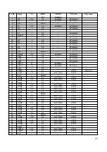
POWER SUPPLY PINS
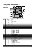
IC301 (SSI3723)
•
Pin Description
INPUT PINS
24
Name
DVDRFP,DVDRFN
RFSIN
AIP, AIN
DIP, DIN
A, B, C, D
A2, B2, C2, D2
CD_A, B, C, D
CD_E, F
MIN
DVDPD
CDPD
LDON
LINK
Description
RF SIGNAL INPUTS: Differential RF signal attenuator input pins.
RF SIGNAL INPUT: Single-ended RF signal attenuator input pin.
AGC AMPLIFIER INPUTS: Differential AGC amplifier input pins.
ANALOG INPUTS FOR RF SINGLE BUFFER: Differential analog inputs to the
RF single-end output buffer and full wave rectifier.
PHOTO DETECTOR INTERFACE INPUTS: Inputs from the main beam Photo
detector matrix outputs.
PHOTO DETECTOR INTERFACE INPUTS: AC coupled inputs for the DPD
from the main beam Photo detector matrix outputs.
CD PHOTO DETECTOR INTERFACE INPUTS : CD_A, B, C, D come from
the CD main beam Photo detector matrix outputs.
CD PHOTO DETECTOR INTERFACE INPUTS: CD side beam photo dector
outputs and used for the CD tracking detection.
RF SIGNAL INPUT FOR MIRROR: AC coupled inputs for the mirror detection
circuit from MEVO.
APC INPUT: DVD APC input pin from the monitor photo diode.
APC INPUT: CD APC input pin from the monitor photo diode.
APC OUTPUT ON/OFF: APC output control pin. A high level activates LD
output. (open low)
LINKING SIGNAL INPUT PIN: In the linking area. This pin goes high and the
Mirror and TE outputs are disabled. When the link signal is enabled. (open low)
Pin No.
1,2
63
59,60
54,55
9, 10, 11, 12
3, 4, 5, 6
13, 14, 15, 16
17, 18
31
23
24
26
33
Type
I
I
I
I
I
I
I
I
I
I
I
I
I


