background image

43

August 2009 Plasma 50PS80

Power Supply Basic Operation

Power Supply Basic Operation

AC Voltage is supplied to the SMPS Board at Connector SC101 from the AC Input assembly. Standby 5V is developed from 
165V source supply (which during run measures 380V measured from the primary fuse F302). 
This supply is also used to generate all other voltages on the SMPS.

The STBY5V (standby) is B+ for the Sub Micon (IC701) on the SMPS and output at P814 pins 11 and 23 then sent to the 
Main PWB for Microprocessor (IC1) operation. AC Detect  is generated on the SMPS, by rectifying a small sample of the  
A/C Line at D102 and associated circuitry and routed to the Sub Micon (IC701) where it outputs at pin 15 and sent to P814 
pin 18 to the Main Board where it is sensed and monitored by the Main Microprocessor (IC1106). If AC Det is missing the 
set will not work. The Main Board will be held in Reset until AC Det returns.
A new feature included on the side keypad is called a Power Button which opens a ground allowing the “Key On” line of 
P814 Pin 24 to go high, turning off the 5V STB line defeating the Micro Processor (IC1106) on the Main Board and Remote 
Control Operation.   

When the Microprocessor (IC1106) on the Main Board receives an “ ON “ Command from either the Power button or the 
Remote IR Signal, it outputs a high called RL ON at Pin 19 of P814. This command causes the Relay Drive Circuit to 
close both Relays RL102 and RL103 bringing the PFC source up to full power by increasing the 165V standby to 380V  
run which can be read measuring voltage at Fuse F302 and F801 from “Hot” Ground.  At this time the run voltages 12V, 
and +5V sources become active and are sent to the Main Board via P814 (12V at pins 5 and 6 and 5V at  pins 9,10, and 
12). The 5V detect line from the Main Board to the SMPS Board can be measured at pin 17 of P814. It is not used.

The next step is for the Microprocessor (IC1106) on the Main Board to output a high on M5V ON Line to the SMPS at P814 
Pin 21 which is sensed by the Sub Micon (IC701) turning on the M5V line and output at P811 and P812 pins 9 and 10  to 
the Y and Z SUS boards and P813 pins 1~4 to the Control board. 

Full Power occurs when the Microprocessor (IC1106) on the Main Board brings the VS-ON line high at Pin 20 of P814 of 
the SMPS Board. VS-ON is routed to the Sub Micon (IC701) which turns on the 17V Audio, VA, and the VS supplies. VA 
and VS output at P811 to the Y-SUS board and P812 to the Z-SUS board. (VA pins 6 and 7 and VS pins 1 and 2 of either 
connector) the 17V Audio supply outputs to the Main board at P814 pins 1 and 2.

AUTO GND Pin 22 of P814: This pin is grounded on the Main board. When it is grounded, the Sub Micon IC701 works in 
the normal mode. Meaning it turns on the power supply via commands sent from the Main board. When this pin is floated 
(opened), it pulls up and turns the Sub Micon IC701 on in the Auto mode. In this state, the Sub Micon turns on the power 
supply in stages automatically. A load is necessary to regulate the 17V with the SMPS disconnected. This is a good test if 
the Main board is suspect.

Содержание 50PS80 Series

Страница 1: ...Advanced Single Scan Troubleshooting Training Manual 50PS80 Plasma Display 50PS80 Plasma Display August 2009 ...

Страница 2: ...d Operation Troubleshooting and Alignment of Switch Mode Power Supply Main Board Section 1 Section 2 Contact Information Preliminary Matters Specifications Plasma Overview General Troubleshooting Steps Disassembly Instructions Voltage and Signal Distribution OUTLINE OUTLINE Power Button Front Key Board NEW Receives its 5V from Power Supply not Y SUS Turns off the SMPS via Key On line NEW ...

Страница 3: ...ve time and money sometimes can be overlooked These techniques will also be presented This Section will get the Technician familiar with the Disassembly Identification and Layout of the Plasma Display Panel At the end of this Section the Technician should be able to Identify the Circuit Boards and have the ability and knowledge necessary to safely remove and replace any Circuit Board or Assembly O...

Страница 4: ...Electronics Unauthorized modifications will not only void the warranty but may lead to property damage or user injury If wires screws clips straps nuts or washers used to complete a ground path are removed for service they must be returned to their original positions and properly fastened CAUTION CAUTION To avoid personal injury disconnect the power before servicing this product If electrical powe...

Страница 5: ...tal device pursuant to Part 15 of the FCC Rules These limits are designed to provide reasonable protection against harmful interference when the equipment is operated in a residential installation This equipment generates uses and can radiate radio frequency energy and if not installed and used in accordance with the instruction manual may cause harmful interference to radio communications However...

Страница 6: ...3 0000 Technical Support and Part Sales 800 847 7597 USA Website GCSC aic lgservice com Customer Service Website us lgservice com LG Web Training lge webex com LG CS Academy lgcsacademy com LG Electronics Alabama Inc 201 James Record Road Huntsville AL 35813 http 136 166 4 200 Published August 2009 by LG Technical Support and Training 32LG40 32LH30 42LG60 42LG70 42LH20 42LH40 42LH50 47LG90 42PG20 ...

Страница 7: ...ed because of residual current stored before Circuit Board removal 4 C MOS circuits are used extensively for processing the Drive Signals and should be protected from static electricity 5 The PDP Module must be carried by two people Always carry vertical NOT horizontal 6 The Plasma television should be transported vertical NOT horizontal 7 Exercise care when making voltage and waveform checks to p...

Страница 8: ... examination using your senses the first check should always be the DC Supply Voltages to those circuits under test Always confirm the supplies are not only the proper level but be sure they are noise free If the supplies are missing check the resistance for possible short circuits Isolate To further isolate the failure check for the proper waveforms with the Oscilloscope to make a final determina...

Страница 9: ...s section of the manual will discuss the specifications of the 50PS80 Single layer design The 1080p Full HD resolution and THX Display certification makes this series the must have HDTV in 2009 PRODUCT INFORMATION PRODUCT INFORMATION ...

Страница 10: ...X Display Certification and THX Cinema Mode THX Media Director Super Bright Panel 1 500 cd m2 Brightness 600Hz Sub Field Driving Four 4 HDMI V 1 3 with Deep Color ISFccc ready USB 2 0 for access to digital music and photos MP3 JPEG LG SimpLink TM Connectivity Smart Energy Saving LG Core Technologies Clear Voice Easy UI menu interface Pure Black Level Auto Navigation VCR DVD Bluray HD DVD SetTop Bo...

Страница 11: ...Chip Key Lock Closed Caption 3 English Spanish French Trilingual Menus English Spanish French EZ Menus High Performance Interface Channel Add Delete Favorite Channel Auto Clock Manual Clock On Off Timer Sleep Timer SimpLink Auto Off When no video is present Image Sticking Minimization 100 000 Hour Panel Life typical NTSC ATSC Tuners with Clear QAM ...

Страница 12: ...OLUTION 1080p HD Resolution Pixels 1920 H 1080 V High definition television is the highest performance segment of the DTV system used in the US It s a wide screen high resolution video image coupled with multi channel compact disc quality sound HDMI 1 3 Deep Color Digital multi connectivity HDMI 1 3 Deep color provides a wider bandwidth 340MHz 10 2Gbps than that of HDMI 1 2 delivering a broader ra...

Страница 13: ...d Band TV Specifications Logo Familiarization Broad Band TV User friendly interface Content service from Yahoo Netflix YouTUBE Widget service from Yahoo Weather VoD shopping and information Yahoo News Yahoo Weather Yahoo Finance Yahoo Video Yahoo Sports Flicker OMG FIXED ...

Страница 14: ...zation Picture Wizard Specifications Logo Familiarization Picture Wizard Customers can customize picture performance without the need for additional expense Picture Wizard easily guides consumers through the calibration process using on screen reference points ...

Страница 15: ...y ensuring clear sound despite loud background noise Save Energy Save Money Home electronic products use energy when they re off to power features like clock displays and remote controls Those that have earned the ENERGY STAR use as much as 60 less energy to perform these functions while providing the same performance at the same price as less efficient models Less energy means you pay less on you...

Страница 16: ...me No smeared images during fast motion scenes 600Hz Sub Field Driving 600Hz Sub Field Driving Note Sub field 2 Note Sub field 2 through 10 are through 10 are actually in reverse actually in reverse Brighter image Brighter image should be last should be last Sub Field firing occurs using wall charge and polarity differences between Y SUS and Z SUS signals ...

Страница 17: ...isplay Certification signifies that an HDTV delivers exceptional images bringing more immersive movie broadcast and video game experiences to your living room Long history in the video category DVD D cinema mastering programs THX Optimizer THX is unique since it is involved in every step of the production chain Mission make the picture at home look like the picture in the studio THX Familiarizatio...

Страница 18: ...18 August 2009 Plasma 50PS80 Remote Control Remote Control TOP PORTION BOTTOM PORTION ...

Страница 19: ...taneously Press and Hold the Menu Key on the Side Key pad and Press and Hold the Menu Key on the Remote approximately 5 seconds 3 If Customer s Menu appears continue to hold until it disappears 4 The Service Menu appears Note It is possible dependant upon the Software Version a Password may be required to enter the Service Menu If a password is required enter 0000 ...

Страница 20: ...20 August 2009 Plasma 50PS80 Rear and Side Input Jacks Rear and Side Input Jacks AC In USB Music Pictures and Software Upgrades LAN also for Software Upgrades ...

Страница 21: ...d you will see COMPLETE 9 Your TV will be restarted automatically CAUTION Do not remove AC power or the USB Flash Drive Do not turn off Power during the upgrade process 2 Copy new software xxx bin to Root Make sure to have correct software file 3 With TV turned on insert USB flash drive 4 You can see the message TV Software Upgrade Shows the Currently Installed Version Shows the Software Version f...

Страница 22: ...and for wall mount Model No Serial No Label 16 5 16 415mm 25 7 16 646mm 32 7 8 835 7mm 6 5 16 160mm 7 7 8 200mm 2 5 16 59 3mm 15 3 4 400mm 5 9 16 140 7mm 15 3 4 400mm 15 3 4 400mm 15 3 4 400mm There must be at least 4 inches of Clearance on all sides 22 82 2 lbs with Stand 75 6 lbs without Stand Weight 282W Typical 0 13W Stand By Power ...

Страница 23: ...Board Identification of the 50PS80 Advanced Single Scan Plasma Display Panel Upon completion of this section the Technician will have a better understanding of the disassembly procedures the layout of the printed circuit boards and be able to identify each board DISASSEMBLY SECTION DISASSEMBLY SECTION ...

Страница 24: ...Cover To remove the back cover remove the 29 screws indicated by the arrows The Stand does not need to be removed PAY CLOSE ATTENTION TO THE TYPE SIZE AND LENGTH Of the screws when replacing the back cover Improper type can damage the front 24 ...

Страница 25: ... X Left X Main PWB Power Supply SMPS PWB FPC FPC Power Button FPC FPC AC In Side Input part of main FPC FPC FPC FPC FPC FPC FPC Center X Z SUB PWB Y Drive Upper Panel Voltage Label Control PWB Panel ID Label Conductive Tape Under Main PWB TCP Heat Sink Control Keys Y Drive Lower Invisible Speakers ...

Страница 26: ...26 August 2009 Plasma 50PS80 SMPS Switch Mode Power Supply PWB Removal SMPS Switch Mode Power Supply PWB Removal P812 P811 P813 SC101 Disconnect P811 P812 P813 and SC101 Then Remove the 8 Screws ...

Страница 27: ... 50PS80 Main PWB Removal Main PWB Removal P1101 Then Remove the 4 Screws P900 n c n c P203 P1108 n c n c Disconnect P1101 P1108 and P900 Disconnect P203 by lifting up the locking mechanism and removing the LVDS ribbon cable ...

Страница 28: ...ing inward on the two locking tabs and rocking the cable out Disconnect P1 P101 P102 and P104 by removing the tape and lifting upward on the locking tab pulling the cable out Then Remove the 4 Screws P101 P5 P104 P102 P2 P200 n c n c n c n c n c n c Look on back Look on back for heat transfer for heat transfer material material ...

Страница 29: ...emoval Disconnect P302 and P307 Disconnect P101 and P309 by removing the tape and lifting upward on the locking tab pulling the cable out Then Remove the 10 Screws Carefully separate the Y SUS from the Y Drive Upper and Lower Boards P302 P101 P307 P309 n c n c ...

Страница 30: ...All connectors Note All connectors going to the Y going to the Y SUS board SUS board are fragile are fragile P114 P116 P214 and P114 P116 P214 and P216 P216 Removing and reinserting Removing and reinserting the drive board or the the drive board or the Y Y SUS can cause an SUS can cause an intermittent or open intermittent or open connection connection Investigate these Investigate these connector...

Страница 31: ...rs Note All connectors going to the Y going to the Y SUS board SUS board are fragile are fragile P114 P116 P214 and P114 P116 P214 and P216 P216 Removing and reinserting Removing and reinserting the drive board or the the drive board or the Y Y SUS can cause an SUS can cause an intermittent or open intermittent or open connection connection Investigate these Investigate these connectors carefully ...

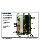
Страница 32: ...emoval Disconnect P100 and P101 Disconnect P102 and P104 by pulling out to the right the locking tabs and removing the FPC from the connector Then Remove the 8 Screws Carefully separate the Z SUS from the Z SUB P103 and remove P104 P102 P103 P101 P100 n c n c ...

Страница 33: ...the bottom of the Power LED PWB Remove the 1 screw at the bottom of the Power LED PWB 1 1 2 2 Note this s Note this screw has an Oversized washer which locks the board in place 2 Ground Strap screw Ground snap Cabinet Bottom Note the left screw in step 1 has a ground strap Note the left screw in step 1 has a ground strap lug Make sure to return it when reinstalling the lug Make sure to return it w...

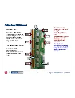
Страница 34: ...1101 and P900 The LVDS connector should already be removed see above D Remove the 4 screws from the Main Board Mounting Bracket Note Decorative Plastic Piece on right does not need to be removed Carefully reposition the Main Board and Mounting Bracket up and off to the right side E Remove the metal support Braces marked E Note There is a Left and a Right brace 3 Screws per bracket F Remove the 13 ...

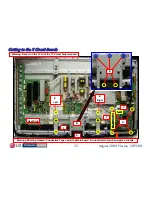
Страница 35: ...X Circuit Boards Getting to the X Circuit Boards A D C E Right E Left F Heat Sink Warning Never run the TV with the TCP Heat Sink removed Warning Shorting Hazard Conductive Tape under the Main board Do not allow to touch energized circuits B B C ...

Страница 36: ...rive Boards At the end of this Section the technician should understand the operation of each circuit board and how to adjust the controls The technician should be able with confidence to troubleshoot a circuit board failure replace the defective circuit and perform all necessary adjustments CIRCUIT OPERATION TROUBLESHOOTING AND CIRCUIT ALIGNMENT SECTION CIRCUIT OPERATION TROUBLESHOOTING AND CIRCU...

Страница 37: ...102 LVDS Y Drive Upper Z SUS PWB P101 P200 P104 P232 P211 P311 P331 Display Panel Vertical Address Color Information Display Panel Grids Address Reset 17V Relay On M5 On VS On STB5V 5V 17V 12V to Main PWB Vs Va and M5V to Y SUS Z SUS M5V to Control PWB SMPS OUTPUT VOLTAGES IN RUN P104 17V Z Drive Signals IR Power LED Intelligent Sensor FPCs FPCs 5V STBY P103 P214 P111 P211 P112 P116 P114 Drive Dat...

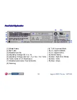
Страница 38: ...ing Voltage Set Up Vy Vsc Ve Vzb 6 Trade name of LG Electronics 7 Manufactured date Year Month 8 Warning Panel Label Explanation Panel Label Explanation 9 TUV Approval Mark 10 UL Approval Mark 11 UL Approval No 12 Model Name 13 Max Watt Full White 14 Max Volts 15 Max Amps 1 2 3 4 5 6 7 8 9 10 11 12 13 14 15 ...

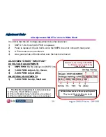
Страница 39: ... Panel is replaced Check Va Vs since the SMPS does not come with new panel 3 A Picture issue is encountered 4 As a general rule of thumb when ever the back is removed Remember the Voltage Label MUST be followed it is specific to the panel s needs All label references are from a specific panel They are not the same for every panel encountered The Waveform adjustment is only necessary 1 When the Y S...

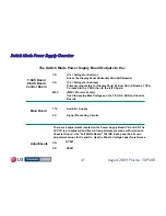
Страница 40: ...er boards The SMPS outputs the following voltages The SMPS outputs the following voltages STBY 5V Stand STBY 5V Stand By 12V 17V to the Main board By 12V 17V to the Main board VS to the Y VS to the Y SUS and Z SUS and Z SUS boards SUS boards VA through Y VA through Y SUS to the X boards for TCPs SUS to the X boards for TCPs M5V to the Control Y M5V to the Control Y SUS and Z SUS and Z SUS boards S...

Страница 41: ...id SUS Boards M5V Monitor 5 volts Used to develop Bias Voltages on the Y SUS Z SUS and Control Boards 17V Audio B Supply 5V Signal Processing Circuits Adjustments There are 2 adjustments located on the Power Supply Board VA and VS The 5V VCC is pre adjusted and fixed All adjustments are made with relation to Chassis Ground Use Full White Raster 100 IRE Each panel has its own adjustment values for ...

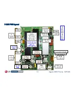
Страница 42: ...trol P814 To Main SK101 Fuse F101 2 15A 250V F302 1A 250V Vs Adj VR901 Va Adj VR501 Hot Ground Symbol M5V M5V Gnd VA VA Gnd Gnd NC VS VS IC701 1 SMPS Switch Mode Power Supply PWB Layout SMPS Switch Mode Power Supply PWB Layout 1 1 1 VS VS NC Gnd Gnd VA VA Gnd M5V M5V 1 4 M5V 5 8 Gnd ...

Страница 43: ...g the PFC source up to full power by increasing the 165V standby to 380V run which can be read measuring voltage at Fuse F302 and F801 from Hot Ground At this time the run voltages 12V and 5V sources become active and are sent to the Main Board via P814 12V at pins 5 and 6 and 5V at pins 9 10 and 12 The 5V detect line from the Main Board to the SMPS Board can be measured at pin 17 of P814 It is no...

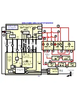
Страница 44: ...1 Watt 6 6 9 In Stand By Primary side is 163V In Run Relay On Primary side is 386V 4 4 14 14 3 3V Reg 2 5V Det Relay On 10 17V 17V 17V 17V 5VFG Va STBY 5V M5V M5V M5V Vs Va Vs Va 15 11 11 11 12 16 16 15 3 3V 12 13 9 15 15 15 5 2 5 Other Circuits Vs Va 13 14 16 10 15 16 10 10 15 15 Standby 5V will not be output if the Power Button is off Power Button On Off Front IR Board Not Used AC Det If missing...

Страница 45: ...ht Set should be in Full White Raster and Heat Run 10 Minutes 1 VS ADJUST Connect DVM to pin 1 or 2 of P812 Adjust VR901 until the voltage matches your panel s voltage label 2 VA ADJUST Connect DVM to pin 6 or 7 of P812 Adjust VR501 until the voltage matches your panel s voltage label VS and VA adjustment resistors are shown in the drawing below VR901 is the VS adjustment pot VR501 is the VA adjus...

Страница 46: ...BY 5V and AC DET should be present 10 M5V 9 M5V 8 Gnd 7 VA 6 VA 5 Gnd 4 Gnd 3 NC 2 VS 1 VS 1 2 3 4 M5V 5 6 7 8 Gnd 100W 100W Pins Check Pin 9 10 12 for 5V Check Pins 1 4 for M5V Check Pins 1 or 2 for 17V Check Pins 5 or 6 for 12V P814 P813 P812 Check Pins 1 or 2 for Vs voltage P811 46 Using two 100 Watt light bulbs attach one end to Vs and the other end to ground Apply AC to SC101 If the light bul...

Страница 47: ...be 4 3V When the Power Button is pressed on the Key On Line is grounded which allows the 5V Standby to go to 5V A Grounding both the Auto Gnd and the Key On Lines will allow the supply to be powered up one section at a time B Add a 100Ω watt resistor from 5V Standby to RL_ON and the 12V and 5V Run Lines will become active C Add a 100Ω watt resistor from 5V Standby to M5V_ON to make the Main 5V Lin...

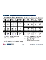
Страница 48: ... 17 3V 0V 17V 1 Diode Mode Run STBY Label Pin Open Gnd Gnd Auto Gnd 22 Open 0V 0V Key On 24 Open 3 2V 0V VS On 20 1 45V 5V 5V AC Det 18 n c n c n c n c 16 Gnd Gnd Gnd Gnd 14 1 2V 5 15V 0V 5V 12 1 2V 5 15V 0V 5V 10 Gnd Gnd Gnd Gnd 8 Open 12V 0V 12V 6 Gnd Gnd Gnd Gnd 4 2 2V 17 3V 0V 17V 2 Diode Mode Run STBY Label Pin P814 CONNECTOR SMPS to Main PWB P1108 Pin 24 When the Power Button is opened Pin 2...

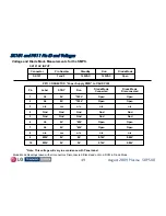
Страница 49: ...th Panel Label 0 74V 5V 0V M5V 10 0 74V 5V 0V M5V 9 n c n c n c n c 8 Open 65V 0V Va 7 Open 65V 0V Va 6 Gnd Gnd Gnd Gnd 5 Gnd Gnd Gnd Gnd 4 n c n c n c n c 3 Open 195V 0V Vs 2 Open 195V 0V Vs 1 Diode Mode Connected Run STBY Label Pin SK101 AC INPUT Standby Run Diode Mode Connector Pin Number SK101 120VAC 120VAC Open 1 and 3 Diode Mode Readings taken with all connectors Disconnected Black lead on G...

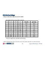
Страница 50: ... will vary in accordance with Panel Label 0 74V 5V 0V M5V 10 0 74V 5V 0V M5V 9 Gnd n c n c n c 8 Open 65V 0V Va 7 Open 65V 0V Va 6 Gnd Gnd Gnd Gnd 5 Gnd Gnd Gnd Gnd 4 n c n c n c n c 3 Open 195V 0V Vs 2 Open 195V 0V Vs 1 Diode Mode Connected Run STBY Label Pin Diode Mode Readings taken with all connectors Disconnected Unless specified Black lead on Gnd DVM in Diode Mode P812 CONNECTOR Power Supply...

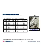
Страница 51: ...nd Gnd Gnd Gnd 7 Gnd Gnd Gnd Gnd 6 Gnd Gnd Gnd Gnd 5 0 75V 5V 0V M5V 4 0 75V 5V 0V M5V 3 0 75V 5V 0V M5V 2 0 75V 5V 0V M5V 1 Diode Mode Connected Run STBY Label Pin Diode Mode Readings taken with all connectors Disconnected Black lead on Gnd DVM in Diode Mode P813 CONNECTOR Power Supply PWB to Control PWB P200 1 NOTE The Black wire on P813 Connector is not pin 1 P813 ...

Страница 52: ...aveform development signals from the Control board The Y waveform development signals from the Control board The Y SUS SUS also develops additional voltages via internal switch mode power also develops additional voltages via internal switch mode power supplies 15V floating ground 5V VSC voltages and supplies 15V floating ground 5V VSC voltages and Vy voltages Vy voltages This board has 4 adjustme...

Страница 53: ...P101 To Control P309 Vy TP R305 FS302 Vs 3A 250V FS303 Va 10A 125V n c Logic Signals in Top 6 pins 17 8V out Set Dn1 Adj VR601 Vy Adj VR902 Set Up1 Adj VR602 P307 To Left X Pins 1 4 Va To Y Drive Upper To Y Drive Lower Vsc TP R306 C324 lower leg Y SUS drive TP 400V p p C323 upper leg Not for Adjustment of the Y Drive signal used to test Y SUS FS301 M5V 4A 125V ...

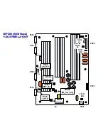
Страница 54: ...nel Y SUS PWB LAYOUT 50PS80 50H3 Panel Y SUS PWB LAYOUT 54 R305 VY TP VR901 VSCAN P309 VR601 SET dn1 VR602 SET up1 R306 VSC TP P312 P311 P313 P314 P101 P302 FS302 Vs FS303 Va FS901 M5V P307 VR902 DD_Var Vy FS301 M5V ...

Страница 55: ...re making adjustments Vs and Va adjustments complete 2 Place unit into White Wash from the Customer s Menu for all adjustments 3 Be sure to use all adjustment values as indicated on your panel s voltage label in the upper right of the panel Example shown above 5 Adjust VSC using VR901 Measured across VSC TPs R306 Match your specific Panel s Voltage label 1V Location Bottom Center Vy VR902 VSC VR90...

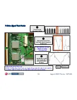
Страница 56: ...form above observed 100uSec div e Highlighted signal from waveforms above observed 50uS div Either test point is OK to use NOTE The Waveform Test Points are fragile If by accident the land is torn and the run lifted make sure there are no lines left to right in the screen picture 50uS 510V p p Y Drive PWB Test Points Middle of bottom Y Drive Board ...

Страница 57: ...aveform Fig 2 At 100us per div the signal for Set Up Down adjustment is now easier to recognize It is outlined within the Waveform Fig 3 At 50uSec per division the adjustment for SET UP or SET DOWN can be made Note When actually performing the adjustments The portion of the waveform being adjusted can be Zoomed in on by increasing the speed of the scope FIG1 2mS FIG2 100uS Outlined Area Blanking F...

Страница 58: ...observing only the peak of the waveform turning the pot CW which cause the peak to dome to the left of the flat portion CCW will cause the peak to decrease in amplitude Turn CW until the dome appears then back off CCW 4 SET DOWN ADJUSTMENT VR601 Adjust VR601 while observing area B and set to 160uSec 5uSec 1 Pre Heat unit for at least 10 Minutes before making adjustments Vs Va Vy and VSC adjustment...

Страница 59: ...w All Waveforms taken at 50V per div 50uSec per div Ramp Vset UP too high Ramp Vset UP too low Vset DN too high Vset DN too low NOTE If Vset DN too high this set will go to excessive bright then shutdown To correct remove the LVDS from control PWB and make necessary adjustments ...

Страница 60: ...ay Panel Power Supply Board SMPS FETs amplify Sustain Waveform Left X Board Z SUS Board Distributes 15V Generates Floating Ground 5V by on board SMPS Logic signals needed to control buffer outputs Routed through Y SUS board Operates referenced to Floating Gnd Center X Board Right X Board Vs and M5V M5V Generates Vsc and Vy from Vs or M5V by internal SMPS Also controls Set Up Down via adj R G B Log...

Страница 61: ...Gnd Open Open Gnd Gnd n c Open Open Diode Mode Disconnected 0 74V 5V M5V 10 0 74V 5V M5V 9 Gnd n c n c 8 Open 65V Va 7 Open 65V Va 6 Gnd Gnd Gnd 5 Gnd Gnd Gnd 4 n c n c n c 3 Open 195V Vs 2 Open 195V Vs 1 Diode Mode Connected Run Label Pin P302 CONNECTOR Y SUS to Power Supply PWB P811 Note This voltage will vary in accordance with Panel Label Voltage and Diode Mode Measurements Note There are no S...

Страница 62: ...ation SUS P307 to Left X Drive P121 Plug Information Gnd Gnd Gnd 7 Gnd Gnd Gnd 6 NC NC NC 5 Open 65V VA 4 Open 65V VA 3 Open 65V VA 2 Open 65V VA 1 Diode Mode Run Label Pin Note This voltage will vary in accordance with Panel Label P307 CONNECTOR Y SUS PWB to X Drive Left P121 Voltage and Diode Mode Measurements Note There are no Stand By Voltages to this board 1 P307 ...

Страница 63: ...d 0 1V Gnd 4 9V Gnd 3 48V 0V Gnd 1 4V Gnd 0 7V Gnd 0 2V Gnd 0 1V Gnd 0 1 0 4V Gnd 4V Gnd 1 15V 2 15V 3 15V 4 15V 5 15V 6 15V 7 NC 8 OC2_ODD 9 GND 10 CLK 11 GND 12 DATA_ODD 13 GND 14 DATA_EVEN 15 16 17 STB 18 GND 19 20 GND GND OC2_EVEN 21 22 GND GND 23 OC1_EVEN 24 GND 25 OC1_ODD GND 26 27 28 29 30 31 32 33 34 35 41 42 43 44 45 46 47 48 49 50 36 37 38 39 40 15V 15V 15V 15V 15V 15V NC OC2_ODD GND CLK...

Страница 64: ...in 1 44V 0 1V ER_DN 45 Gnd Gnd GND 46 1 44V 0 1 0 4V SUS_UP 47 Gnd Gnd GND 48 1 44V 4V SUS_DN 49 Gnd Gnd GND 50 Gnd Gnd GND 44 1 44V 0 2V ER_UP 43 Gnd Gnd GND 42 1 44V 0 7V DELTA_VY2 41 Gnd Gnd GND 40 1 44V 1 4V PASS_TOP 39 Gnd Gnd GND 38 1 44V 0V CTRL_OE 37 1 44V 3 48V SET_DN1 36 Gnd Gnd GND 35 1 44V 4 9V SET_DN2 34 Gnd Gnd GND 33 1 44V 0 1V SET_UP1 32 Gnd Gnd GND 31 1 44V 0V SET_UP2 30 Gnd Gnd G...

Страница 65: ...eter is in Diode Mode 1 1 Red Lead 0 6V Red Lead 0 6V Black Lead 0 5V Black Lead 0 5V Note All connectors going to the Y Note All connectors going to the Y SUS board are fragile SUS board are fragile P114 P116 P214 and P216 P114 P116 P214 and P216 Removing and reinserting the drive board or the Y Removing and reinserting the drive board or the Y SUS can SUS can cause an intermittent connection or ...

Страница 66: ...n Label Pin Note All Voltage Measurement taken from Floating Ground 2 7V 140V VScan 11 12 n c n c n c 10 1 3V 5V 5VFG 8 9 FGnd FGnd FGnd 1 7 Diode Mode Run Label Pin Voltage and Diode Check Measurements This board has no Stand By voltage All Pins are Floating Ground P312 CONNECTOR Y SUS to Upper Y Drive P114 All Pins are Floating Ground P314 CONNECTOR Y SUS to Lower Y Drive P216 P313 CONNECTOR Y S...

Страница 67: ...0 horizontal electrodes These boards have no DC adjustments These boards receives their main B from the Y These boards receives their main B from the Y SUS PWB SUS PWB Floating ground 5V from the Switched Mode Power Floating ground 5V from the Switched Mode Power Supply on the Y Supply on the Y SUS board SUS board Must be measured from the Floating Ground Must be measured from the Floating Ground ...

Страница 68: ...ors going to the Y going to the Y SUS SUS board are fragile board are fragile P114 P116 P114 P116 P214 and P216 P214 and P216 Removing and Removing and reinserting the drive reinserting the drive board or the Y board or the Y SUS can SUS can cause an intermittent cause an intermittent connection or cold connection or cold connection connection Investigate these Investigate these connectors careful...

Страница 69: ...ignals for lower drive board lower drive board Y Drive V Scan signal in Y Drive V Scan signal in on bottom two pins 1 and 2 on bottom two pins 1 and 2 Y Drive V Scan signal Y Drive V Scan signal in on top two pins 11 and 12 in on top two pins 11 and 12 All Pins Floating Ground All Pins Floating Ground All Pins Floating Ground All Pins Floating Ground Floating Ground 5V pins 8 and 9 Floating Ground...

Страница 70: ...e When removing either Note When removing either Y Y Drive board these Drive board these Chocolate pieces will Chocolate pieces will Stick Stick making the board feel as making the board feel as thought its still attached thought its still attached Note the PWB stand Note the PWB stand off The off The top of the stand top of the stand off has a off has a collar which enters the PWB collar which en...

Страница 71: ...nder either end object under either end of the FPC and lift up of the FPC and lift up gently releasing the tab gently releasing the tab Tab Tab Tab Tab Gently pull the FPC Gently pull the FPC from the connector from the connector When reinserting the When reinserting the FPC make certain that FPC make certain that both tabs are seated both tabs are seated correctly before correctly before attempti...

Страница 72: ...ing Gnd Checked from Floating Gnd Y Drive Upper P116 Y Drive Upper P116 Y Drive Upper P214 Y Drive Upper P214 Floating Floating Ground Ground 5V FG 5V FG VSCAN VSCAN n c n c Floating Floating Ground Ground 5V FG 5V FG VSCAN VSCAN n c n c BL 0 60V BL 0 60V RL RL Open Open 5V FG 5V FG VSCAN VSCAN Diode Check means the Digital Volt Meter is in Diode Mode all connectors to PWB are removed 1 1 These ar...

Страница 73: ...n Label Pin Note All Voltage Measurement taken from Floating Ground Open 140V VScan 11 12 n c n c n c 10 Open 5V 5VFG 8 9 FGnd FGnd FGnd 1 7 Diode Mode Run Label Pin Voltage and Diode Check Measurements This board has no Stand By voltage All Pins are Floating Ground P114 CONNECTOR Upper Y Drive to Y SUS P312 All Pins are Floating Ground P216 CONNECTOR Lower Y Drive to Y SUS P314 P214 CONNECTOR Low...

Страница 74: ...L Red Lead on test point black lead on FG BL 0 76V BL 0 76V RL RL Open Open BL 0 87V BL 0 87V BL 0 87V BL 0 87V BL 0 85V BL 0 85V BL 0 85V BL 0 85V BL 0 87V BL 0 87V BL 0 84V BL 0 84V BL 0 84V BL 0 84V BL 0 87V BL 0 87V BL 0 87V BL 0 87V BL 0 87V BL 0 87V BL 0 85V BL 0 85V BL 0 85V BL 0 85V BL 0 84V BL 0 84V BL 0 87V BL 0 87V All readings Open with All readings Open with RL RL All All readings rea...

Страница 75: ...und 5V Floating Ground BL 0 6V BL 0 6V RL RL Open Open Diode Mode Check All checks from Floating Gnd BL Black Lead on test point red lead on FG RL Red Lead on test point black lead on FG BL 0 76V BL 0 76V RL RL Open Open BL 0 84V BL 0 84V BL 0 84V BL 0 84V BL 0 87V BL 0 87V BL 0 87V BL 0 87V BL 0 84V BL 0 84V BL 0 84V BL 0 84V BL 0 87V BL 0 87V BL 0 87V BL 0 87V All readings Open with All readings...

Страница 76: ...on the left are actually the bottom connections on the Flexible bottom connections on the Flexible Ribbon Cable to the Panel FPC The Ribbon Cable to the Panel FPC The top connections to the FPC are on top top connections to the FPC are on top of the board as shown on the right of the board as shown on the right Back Side of Y Drive board Back Side of Y Drive board Front Side of Y Drive board Front...

Страница 77: ...lops the SUS board develops the Panel Erase Panel Erase Sustain Signals Sustain Signals This board has one DC adjustment Z This board has one DC adjustment Z Bias Bias Board Receives its main B from the Board Receives its main B from the VS from the Switched Mode Power Supply VS from the Switched Mode Power Supply 15V from the Control board but developed on the 15V from the Control board but devel...

Страница 78: ...out Z Bias Adj VR201 P312 To SMPS P103 To Z Sub Z Bias TP R457 Top Side to Chassis Gnd P301 nc P100 To Control VS VS NC GND GND VA VA NC M5V M5V Pins 1 4 17 8V FS102 Vs 3A 250V FS100 5V 4A 125V P104 To Panel P102 To Panel Z Drive TP FL103 No IPMs No IPMs Z SUS ...

Страница 79: ...or all adjustments 3 Be sure to use all adjustment values as indicated on the panel voltage label in the upper right hand corner of the panel Example above PROCEDURE See preceding page for locations 4 Place DC Volt meter on VZB TP Top of R457 to Chassis Gnd 5 Adjust VZB Z Bias VR201 to match your specific Panel s voltage label Z Bias ADJ VR201 Z Bias TP Top of R457 to Chassis Gnd Lower Right Side ...

Страница 80: ... SUS and Z SUS From the Waveform it can be seen that the timing of the Z SUS must align to the Y SUS for the panel to work correctly If the timing is out of sync the Control board is at fault Note While making adjustments to the Ramp Up and or Rame Down portion of the Y Drive signal the Control board makes the same adjustments to the Z SUS waveform ...

Страница 81: ... the 17V from pin 1 or pin 2 P814 to the Z SUS connector P100 1 5 4 Place the Scope on the Z SUS waveform Test Point FL103 5 Confirm there is an Output from the Z SUS PWB approximate 230V p p This test confirms that the Power Supply Control Board and Z SUS boards are all working OK Light bulbs must remain connected to the Vs from the Power Supply to Gnd Failure to do so will cause the 17V to fluxu...

Страница 82: ...connectors Disconnected unless specified Black lead on Gnd DVM in Diode Mode P101 CONNECTOR Z SUS PWB to Power Supply P812 Open Open Gnd Open Open Gnd Gnd n c Open Open Diode Mode Disconnected 0 74V 5V M5V 10 0 74V 5V M5V 9 Gnd n c n c 8 Open 65V Va 7 Open 65V Va 6 Gnd Gnd Gnd 5 Gnd Gnd Gnd 4 n c n c n c 3 Open 195V Vs 2 Open 195V Vs 1 Diode Mode Connected Run Label Pin Note This voltage will vary...

Страница 83: ...en 0V ER UP 6 Open 0V CTRL OE 5 1 9V 17 8V 15V 4 1 9V 17 8V 15V 3 1 9V 17 8V 15V 2 1 9V 17 8V 15V 1 Diode Mode Run Label Pin Diode Mode Readings taken with all connectors Disconnected Black lead on Gnd DVM in Diode Mode P100 CONNECTOR Z SUS PWB to Control Board P2 1 Note Black wire is NOT pin 1 Voltage and Diode Mode Measurements for the Z SUS PWB This board has no Stand By voltages ...

Страница 84: ... product a pattern on the tern on the screen for testing purposes This can be done without the Main b screen for testing purposes This can be done without the Main board oard delivering LVDS video to confirm if the problem lies with the Ma delivering LVDS video to confirm if the problem lies with the Main board or in board or the panel and its boards the panel and its boards The Control Board Rece...

Страница 85: ...P2 To Z SUS IC7 IC1 P101 To Left X Top 6 pins 17 8V in P102 To Center X P104 To Right X P5 LVDS P200 To SMPS P202 n c IC16 IC304 P6 Auto Gen Short 1 2 IC12 Pins 1 4 5V P3 n c X2 50Mhz FL4 5V FL5 5V D7 Data D6 Temp 1 1 1 3 3V FOR TCPs Pins 1 4 To each X Board Pins 1 4 3 3V Pins 1 4 3 3V Pins 1 4 3 3V ...

Страница 86: ... FL5 5V The two EMI Filters just below P200 are surface mount mini devices which shunt high frequencies to ground They have 4 pins The top and bottom are the B route the two side solder points are Chassis Gnd Gnd 5V Gnd 5V FL4 or FL5 5V EMI filters P200 1 NOTE The Black wire on P200 Connector is not pin 1 ...

Страница 87: ...issing the Control board can still be tested If the ll be tested If the SMPS is developing STBY 5V the STBY 5V can be jumped to any 5V SMPS is developing STBY 5V the STBY 5V can be jumped to any 5V point on the point on the Control board Confirm that LED D6 and LED D7 are illuminated or Control board Confirm that LED D6 and LED D7 are illuminated or blinking if they blinking if they are the board ...

Страница 88: ...88 August 2009 Plasma 50PS80 Control Board Crystal X2 Check Control Board Crystal X2 Check 50Mhz 4V P P Use bottom left leg of Crystal ...

Страница 89: ...rd supplies Video Signals to the TCP Tape Carrier Package ICs If there is a bar defect on the screen it could be a Control Board problem MCM 16 bit 256 Lines output Total Control Board to X Board Address Signal Flow IC1 Control PWB Signal Block Control PWB Signal Block MCM IC1 DRAM 2 Buffers per TCP CONTROL PWB X DRIVE PWB PANEL 128 Lines per Buffer EEPROM 23 Total TCPs 5888 Line Outputs RGB per P...

Страница 90: ...g are too close together for safe readings use Test Points To remove the LVDS cable press the two locking tabs inward then rock the connector side to side while pulling out on the connector If a video problem is encountered to eliminate all Panel boards remove the LVDS cable and then jump the Auto Gen connector pin 1 and 2 If the picture is OK the Power Supply Y SUS Z SUS Y Drives X Boards TCPs an...

Страница 91: ...V 0V 2 Diode Mode Run Pin 15 15 5 5 2 2 Open 3 3V 42 Open 3 3V 40 Open 3 3V 41 Open 1 1V 38 Open 1 2V 39 1 3V 1 1V 35 1 3V 1 2V 36 Open 0 58V 43 1 3V 1 2V 33 1 3V 1 1V 32 1 3V 1 1V 31 1 3V 1 2V 30 1 3V 1 1V 29 1 3V 1 2V 28 1 3V 1 2V 27 1 3V 1 1V 26 1 3V 1 2V 25 Diode Mode Run Pin P5 Connector Control Board to Main PWB P203 Note There are no voltages in Stand By mode Gnd Gnd P5 20 20 25 25 30 30 35...

Страница 92: ...ode 1 32V 17 8V 15V 10 1 32V 17 8V 15V 11 1 32V 17 8V 15V 12 1 32V 17 8V 15V 9 1 4V 0V CTRL OE 8 1 48V 0V ER UP 7 1 48V 0V ER DN 6 Gnd Gnd Gnd 5 1 48V 3V Z Bias 4 1 49V Gnd Gnd 3 1 49V 0 4V SUS UP 2 1 49V 0 7V SUS DN 1 Diode Mode Run Label Pin Diode Mode Readings taken with all connectors Disconnected Black lead on Gnd DVM in Diode Mode P2 CONNECTOR Control Board to Z SUS PWB P100 1 1 P2 Label P2 ...

Страница 93: ...6 Gnd Gnd Gnd 5 0 75V 5V M5V 4 0 75V 5V M5V 3 0 75V 5V M5V 2 0 75V 5V M5V 1 Diode Mode Connected Run Label Pin Diode Mode Readings taken with all connectors Disconnected Unless Specified Black lead on Gnd DVM in Diode Mode P200 CONNECTOR Control PWB to Power Supply PWB P813 1 Voltage and Diode Mode Measurements for the Control PWB Note There are no voltages in Stand By mode NOTE The Black wire on ...

Страница 94: ...8 39 40 15V 15V 15V 15V 15V 15V NC OC2_ODD GND CLK GND DATA_ODD GND DATA_EVEN STB GND GND GND OC2_EVEN GND GND OC1_EVEN DELTA_VY_ON_OFF GND GND DELTA_VY1 GND SET_UP2 GND SET_UP1 GND SET_DN2 GND DELTA_VY2 GND ER_UP GND ER_DN GND SUS_UP GND SUS_DN GND SET_DN1 CTRL_OE GND PASS_TOP GND OC1_ODD GND P101 Y SUS PWB P1 Control PWB 17 8V 17 8V 17 8V 17 8V 17 8V 17 8V NC 2 84V Gnd 1 87V Gnd 0 3V Gnd 0V Gnd ...

Страница 95: ...Run Label Pin 1 44V 0 1V ER_DN 45 Gnd Gnd GND 46 1 44V 0 1 0 4V SUS_UP 47 Gnd Gnd GND 48 1 44V 4V SUS_DN 49 Gnd Gnd GND 50 Gnd Gnd GND 44 1 44V 0 2V ER_UP 43 Gnd Gnd GND 42 1 44V 0 7V DELTA_VY2 41 Gnd Gnd GND 40 1 44V 1 4V PASS_TOP 39 Gnd Gnd GND 38 1 44V 0V CTRL_OE 37 1 44V 3 48V SET_DN1 36 Gnd Gnd GND 35 1 44V 4 9V SET_DN2 34 Gnd Gnd GND 33 1 44V 0 1V SET_UP1 32 Gnd Gnd GND 31 1 44V 0V SET_UP2 3...

Страница 96: ...0 97V 1 0V 6 0 67V 3 3V 1 4 Diode Mode Run Pin Leave Connector P101 Connected to the X Board P110 Pins with no TP are Gnd 1 4 1 4 6 6 11 11 20 20 31 31 40 40 56 56 0 97V 1 0V 53 0 97V 1 27V 54 1 2V 1 87V 56 1 2V 1 87V 57 1 2V 3 22V 58 1 1V 0 49V 59 0 97V 1 27V 52 0 97V 1 27V 50 0 97V 1 0V 51 0 97V 1 27V 47 0 97V 1 0V 49 0 97V 1 27V 45 0 97V 1 0V 46 1 1V 0 49V 60 0 97V 1 0V 44 0 97V 1 27V 42 0 97V ...

Страница 97: ...P are Gnd 0 97V 1 27V 21 0 97V 1 0V 22 0 97V 1 0V 33 0 97V 1 27V 34 0 97V 1 0V 36 0 97V 1 27V 31 0 97V 1 0V 30 0 97V 1 27V 28 0 97V 1 0V 27 0 97V 1 27V 25 0 97V 1 0V 24 Diode Mode Run Pin 0 97V 1 27V 37 0 97V 1 0V 39 0 97V 1 27V 40 0 97V 1 0V 42 0 97V 1 27V 46 0 97V 1 0V 48 0 97V 1 27V 49 0 97V 1 0V 51 0 97V 1 27V 52 0 97V 1 0V 45 0 97V 1 27V 43 Diode Mode Run Pin 0 97V 1 0V 53 0 97V 1 27V 54 1 2V...

Страница 98: ... 6 0 67V 3 3V 1 4 Diode Mode Run Pin 1 4 1 4 6 6 10 10 20 20 40 40 56 56 Leave Connector P104 Connected to the X Board P310 Note There are no voltages in Stand By mode Pins with no TP are Gnd 60 60 0 98V 1 0V 53 0 98V 1 27V 54 0 49V 1 87V 56 0 49V 1 87V 57 3 22V 3 22V 58 1 87V 0 49V 59 0 98V 1 27V 52 0 98V 1 27V 50 0 98V 1 0V 51 0 98V 1 27V 47 0 98V 1 0V 49 0 98V 1 27V 45 0 98V 1 0V 46 1 87V 0 49V...

Страница 99: ... are the attachment points for these FPCs points for these FPCs These boards have no adjustment These boards have no adjustment These boards receive their main B from the These boards receive their main B from the Originally developed on the Switched Mode Power Supply Originally developed on the Switched Mode Power Supply Va Voltage for Address is routed through the Y Va Voltage for Address is rou...

Страница 100: ...e Center X sends Va to the Righ Va to the Center X and then the Center X sends Va to the Right X t X They route the Logic Color signals from the Control board They route the Logic Color signals from the Control board to all of the Taped Carrier Packages TCPs Including to all of the Taped Carrier Packages TCPs Including VPP VPP which is which is generated on each of the 3 X boards generated on each...

Страница 101: ...ve one TCPs have one heat sink across heat sink across all 23 TCPs as all 23 TCPs as indicated by the indicated by the arrow arrow NEVER run the television with this heat sink removed NEVER run the television with this heat sink removed Damage to the TCPs will occur and cause a defective panel Damage to the TCPs will occur and cause a defective panel ...

Страница 102: ...ds have two similar circuit layouts for the connections going to the TCPs as shown below On any Va 0 54V TCPs connected On any Va 0 84V TCPs disconnected On 3 3V 0 42V On any VPP 0 42V On any Gnd On the below On any Va Open On 3 3V 0 62V On any VPP Open On any Gnd On the below Readings given with TCPs connected unless specified ...

Страница 103: ...xible Cable Y SUS Board Va Logic Connector X Drive Board Heat Sink 128 lines 128 lines 256 total lines There are a total of 23 TCP ICs on the 50H3 panel 8 on the left and right X boards and 7 connected to the center X board Each TCP is supplied with 16 bit RGB data and decodes it to the Panel by connecting the PAD Electrode of the PANEL with the TCP and the TCP with the X Board 1920 Horizontal 588...

Страница 104: ...ny TCPs being discolored Ribbon Damage Cracks folds Pinches scratches etc On any Gnd On any Va 0 58V On 3 3V 0 72V On any VPP 0 58V Reverse leads reads Open 10 15 20 25 30 35 40 45 50 1 Va Va Gnd Gnd VPP VPP 3 3V Gnd Must be checked on flexible cable On the below 5 ...

Страница 105: ... PWB P310 Center X PWB P210 For Connectors P101 P102 and P104 on the Control board see Control board section 3 3V for TCPs IC304 on Control Board All Connectors to All TCPs look very similar for the 3 3V test point The upside down L trace at pins 34 and 35 of each connector Example here from P204 You can only check for continuity you can not run the set with heat sink removed Red Lead On 3 3V 0 42...

Страница 106: ...o shutdown b Generate abnormal vertical bars c Cause the entire area driven by the TCP to be All White d Cause the entire area driven by the TCP to be All Black e Cause a Single Line defect Warning DO NOT attempt to run the set with the Heat Sink over the TCPs removed After a very short time these ICs will begin to self destruct due to overheating ...

Страница 107: ... Left X Drive P121 Connector to Y SUS P307 Information SUS P307 Information Gnd Gnd Gnd 7 Gnd Gnd Gnd 6 NC NC NC 5 Open 65V VA 4 Open 65V VA 3 Open 65V VA 2 Open 65V VA 1 Diode Mode Run Label Pin Note This voltage will vary in accordance with Panel Label P121 CONNECTOR X Drive Left PWB to Y SUS P307 Voltage and Diode Mode Measurement No Stand By Voltages 1 ...

Страница 108: ...Pin Leave Connector P310 Connected to the Control Board P104 0 67V 3 3V 57 60 0 97V 1 0V 55 0 97V 1 27V 54 0 97V 1 0V 53 0 97V 1 27V 52 0 97V 1 0V 50 0 97V 1 27V 49 0 97V 1 0V 48 0 97V 1 27V 47 0 97V 1 0V 46 0 97V 1 27V 45 0 97V 1 0V 43 0 97V 1 27V 42 0 97V 1 0V 41 0 97V 1 27V 40 0 97V 1 0V 38 0 97V 1 27V 37 0 97V 1 0V 35 0 97V 1 27V 34 0 97V 1 0V 33 0 97V 1 27V 32 0 97V 1 0V 30 0 97V 1 27V 29 Dio...

Страница 109: ... 49V 1 Diode Mode Run Pin Leave Connector P210 Connected to the Control Board P102 0 67V 3 3V 57 60 0 97V 1 0V 55 0 97V 1 27V 54 0 97V 1 0V 53 0 97V 1 27V 52 0 97V 1 0V 50 0 97V 1 27V 49 0 97V 1 0V 48 0 97V 1 27V 47 0 97V 1 0V 46 0 97V 1 27V 45 0 97V 1 0V 43 0 97V 1 27V 42 0 97V 1 0V 41 0 97V 1 27V 40 0 97V 1 0V 38 0 97V 1 27V 37 0 97V 1 0V 35 0 97V 1 27V 34 0 97V 1 0V 33 0 97V 1 27V 32 0 97V 1 0V...

Страница 110: ...0 97V 1 27V 16 0 97V 1 0V 15 0 97V 1 27V 14 0 97V 1 0V 12 0 97V 1 27V 11 0 97V 1 0V 10 0 97V 1 27V 9 0 97V 1 0V 8 0 97V 1 27V 7 1 2V 1 87V 5 1 2 1 87V 4 1 2V 3 22V 3 1 1V 0 49V 2 1 1V 0 49V 1 Diode Mode Run Pin 0 67V 3 3V 57 60 0 97V 1 0V 55 0 97V 1 27V 54 0 97V 1 0V 53 0 97V 1 27V 52 0 97V 1 0V 50 0 97V 1 27V 49 0 97V 1 0V 48 0 97V 1 27V 47 0 97V 1 0V 46 0 97V 1 27V 45 0 97V 1 0V 43 0 97V 1 27V 4...

Страница 111: ...ter X Right X P221 P320 16 18 16 18 nc nc On any Va 0 54V TCPs connected On any Va 0 84V TCPs disconnected On any Gnd On any Va Open TCPs connected or disconnected On any Gnd Note Va voltage will vary by panel check your specific panel Note Va voltage will vary by panel check your specific panel s voltage label s voltage label 1 15 1 15 Gnd Gnd 16 30 16 30 Gnd Gnd 13 15 13 15 nc nc 1 12 1 12 Va Va...

Страница 112: ...oard via the LVDS cable The main tuner r VSB VSB 8VSB and QAM is located on the main board This board is also w 8VSB and QAM is located on the main board This board is also where the here the television television s software upgrades are accomplished through the USB input s software upgrades are accomplished through the USB input This board has no adjustment This board has no adjustment The Main B...

Страница 113: ...ut Main PWB Layout IC100 Video Processor X300 X1102 IC1106 Micro P203 To Control P1101 To Ft Control P201 N A Tuner 19 1 LAN HDMI Micro Reset P1111 N C Video Reset IC900 Audio Amp IC801 HDMI P900 To Speakers P1108 To SMPS Video TPs IC1005 IC1008 ...

Страница 114: ...7 Reset 1 2V Core B A2 5V Regulator 3 4V Regulator Q1004 5V B Source 0 12V 5V 5V 5V 3 3V 0 12V IC601 IC802 A C C S G D B IC900 E C B E B C Q500 Q501 IC602 Q602 E C B B C E E C B C A Q202 Q201 D1010 Q900 Q901 IC601 1 Gnd 2 1 8V 3 3 3V C C C C C C C B B B B B B B E E E E E E E Q707 Q709 Q706 Q708 Q703 Q704 Q705 IC1018 IC103 IC1107 Q801 D801 Q801 S 2 5V G 3 3V D 3 2V B 2 5V S D G S D G TUNER TU503 TD...

Страница 115: ...IN PWB Crystal Location Main PWB Crystal X1 and X501 Check Main PWB Crystal X1 and X501 Check X1102 3 5V p p 10Mhz X300 980mV p p 54Mhz X1102 Runs all the time X300 Runs only when set is on Use bottom leg of L300 to measure L300 X300 ...

Страница 116: ...ns Exposed TDVW Main PWB Tuner Check Shield Off Pins Exposed TDVW H103F H103F Video Pin 19 Video Test Point SIF Pin 16 Audio Test Point Pin 4 Tuner B 5V Pin 1 DIG IF Pin 13 DIG IF Pin 12 Digital Channel Test Point Data Pin 9 Clock Pin 8 TU501 MAIN PWB Tuner Location ...

Страница 117: ...utput Check Tuner Location 450mVp p Pin 19 Video Signal Pin 16 SIF Signal 2 24Vp p USING COLOR BAR SIGNAL INPUT Pin 12 and Pin 13 Dig IF Signal Note Dig IF Signal only when receiving a Digital Channel 100mV 1uSec Pin 1 Note Video Out Signal only when receiving an analog Channel 700mVp p 200mV 2uSec 500mV 10uSec ...

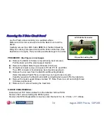
Страница 118: ...g tab is very thin and fragile its best to lift Since the locking tab is very thin and fragile its best to lift slightly one end then work across the locking tab slightly one end then work across the locking tab a little at a time back and forth until the tab is released a little at a time back and forth until the tab is released 2 Remove the ribbon cable from the connector 2 Remove the ribbon cab...

Страница 119: ... PWB Main PWB P203 LVDS Video Signal Check Location Identified Main PWB P203 LVDS Video Signal Check Location Identified Video TP Location Video TPs Numbers relate to P203 Pin Numbers 28 28 11 11 27 27 12 12 21 21 22 22 17 17 16 16 P203 ...

Страница 120: ...Plasma 50PS80 Main PWB P203 LVDS Video Signal Check Main PWB P203 LVDS Video Signal Check Pins 21 22 27 and 28 Pins 21 22 27 and 28 Pin 28 SMTP Color Bar Signal Input Waveform TP see previous page Pin 27 Pin 22 Pin 21 ...

Страница 121: ...lasma 50PS80 Main PWB P203 LVDS Video Signal Check Main PWB P203 LVDS Video Signal Check Pins 11 12 16 and 17 Pins 11 12 16 and 17 SMTP Color Bar Signal Input Waveform TP Under the LVDS Cable Pin 17 Pin 16 Pin 12 Pin 11 ...

Страница 122: ...122 August 2009 Plasma 50PS80 Main PWB Main PWB Semiconductor Semiconductor Component Component Voltages Voltages ...

Страница 123: ... 17 3V 0V 17V 1 Diode Mode Run STBY Label Pin Open Gnd Gnd Auto Gnd 22 Open 0V 0V Key On 24 Open 3 2V 0V VS On 20 1 45V 5V 5V AC Det 18 n c n c n c n c 16 Gnd Gnd Gnd Gnd 14 1 2V 5 15V 0V 5V 12 1 2V 5 15V 0V 5V 10 Gnd Gnd Gnd Gnd 8 Open 12V 0V 12V 6 Gnd Gnd Gnd Gnd 4 2 2V 17 3V 0V 17V 2 Diode Mode Run STBY Label Pin P1108 CONNECTOR Main PWB to P814 SMPS Pin 24 When the Power Button is opened Pin 2...

Страница 124: ... Gnd Open 0V 0V 4 3V Key On 5 1 9V 3 3V 3 3V Key2 4 1 9V 3 3V 3 3V Key1 3 Gnd Gnd Gnd Gnd 2 2V 3 98V 4V IR 1 Diode Check Run STBY Label Pin Diode Mode Readings taken with all connectors Disconnected Black lead on Gnd DVM in Diode Mode P1101 1 Stand By 5V This TV has a center LED which also turns on then goes off after turn on 7 8 Intelligent Sensor Pin 5 Power Key This pin is 0V when the button is...

Страница 125: ...Main PWB Speaker Plug P900 Main PWB Speaker Plug P900 P900 Speaker Connector Diode Mode Check with the PWB Disconnected DVM in the Diode mode L L R R Label Open 8 65V 0V 4 Open 8 65V 0V 3 Open 8 65V 0V 2 Open 8 65V 0V 1 Diode Mode Run SBY Pin MAIN PWB Board Location P1005 CONNECTOR Main to Speakers ...

Страница 126: ...B The front Intelligent Sensor IC communicates with the Main PWB Microprocessor via Clock and Data lines Microprocessor via Clock and Data lines These boards have no adjustments These boards have no adjustments The Front Control Board IR and Intelligent Sensor receives its The Front Control Board IR and Intelligent Sensor receives its main main B from the Main PWB B from the Main PWB STBY 5V from ...

Страница 127: ...127 August 2009 Plasma 50PS80 Front Control PWB Layout Front Control PWB Layout J1 J2 Lower Left Side As viewed from rear Lower Left Side As viewed from rear ...

Страница 128: ...ew To remove the Ft Power LED To remove the Ft Power LED and Ft IR board and Ft IR board Remove the two screws Remove the two screws from the Right Tweeter from the Right Tweeter Drop it out of the way Drop it out of the way Remove the 2 screws in the Remove the 2 screws in the Front IR PWB and the 1 Front IR PWB and the 1 screw at the bottom of the screw at the bottom of the Power LED PWB Power L...

Страница 129: ...LED and IR Board Layout Front Power LED and IR Board Layout Power LED PWB Front IR PWB Right Tweeter P2 P1 P3 J1 J2 Intelligent Sensor IR Sensor Power LEDs Center LED PWB Location Dead center under Panel From Power LED PWB P3 to Center LED PWB ...

Страница 130: ...tor Layout Power LED PWB front Front IR PWB P2 P1 P3 J1 J2 Power LEDs Power LED PWB back Green Red Stand By Green Green LEDs turn on when power first turned on Then they get brighter then they go off P3 connector receives the Center LED control signal from pin 15 of P1 and then delivers it to the Center LED PWB ...

Страница 131: ...131 August 2009 Plasma 50PS80 Front IR and Intelligent Sensor Board Layout Front IR and Intelligent Sensor Board Layout Intelligent Sensor U2 Infrared Sensor U1 Ft View ...

Страница 132: ... 0 56V 5V 11 1 25V 5V 5V STBY 5V 10 Gnd Gnd Gnd Gnd 9 2V 3 3V 3V EYEQ SDA 8 2V 3 3V 3V EYEQ SCL 7 Gnd Gnd Gnd Gnd 6 Gnd Open 0V 0V 4 3V Key On 5 1 9V 3 3V 3 3V Key2 4 1 9V 3 3V 3 3V Key1 3 Gnd Gnd Gnd Gnd 2 2V 3 98V 4V IR 1 Diode Check Run STBY Label Pin Stand By 5V This TV has a center LED which also turns on then goes off after turn on 7 8 Intelligent Sensor Pin 5 Power Key This pin is 0V when t...

Страница 133: ...ges and Pin Identification n Gnd Gnd 3 3V 3 3V STBY2 Gnd Gnd Gnd 4 Open Gnd 4 38V 3 Open 3 3V 0V 2 Open 3 3V 0V 1 Diode Mode Run STBY1 Pin J2 CONNECTOR Ft IR PWB to Ft Key STBY2 Main Power Button is IN STBY1 Main Power Button is OUT Diode Mode Readings taken with all connectors Disconnected Black lead on Gnd DVM in Diode Mode For Voltages when each Key is pressed see the Key PWB section ...

Страница 134: ...134 August 2009 Plasma 50PS80 Side Key Assembly Side Key Assembly c To Ft IR PWB P1 SW8 SW2 SW6 SW7 SW4 SW5 SW3 SW1 c ...

Страница 135: ...easurements with Key pressed P1 Connector Side Key to IR LED Control PWB J2 No Key Pressed Gnd PWR SW KEY 2 KEY 1 Gnd Gnd 3 3V 3 3V STBY2 Open Gnd Gnd 4 Open Gnd 4 38V 3 Open 3 3V 0V 2 Open 3 3V 0V 1 Diode Mode Run STBY1 Pin STBY1 PWR SW Out STBY2 PWR SW In Diode Mode Readings taken with all connectors Disconnected Black lead on Gnd DVM in Diode Mode Menu Enter Volume Volume KEY 1 56V 2 2V 0 19V 0...

Страница 136: ...eet drawing drawing This drawing is a quick reference single sheet drawing with with references to many of the repair tips voltages and layouts givi references to many of the repair tips voltages and layouts giving ng during the presentation during the presentation The 11 X 17 foldout is best viewed in the Adobe version in which The 11 X 17 foldout is best viewed in the Adobe version in which the ...

Страница 137: ...rsed from P100 LOC Source Gate Q901 140V 144V Q903 85V Drain 163V 275V 88V 0 86V Open NC 6 7 8 9 10 Diode Check Pin Diode Check Pin NC Open Gnd 1 2 3 4 5 1 2 pins Y Drive Logic Sig P110 3 3V in on Pins 57 60 P210 3 3V in on Pins 57 60 P310 3 3V in on Pins 57 60 P320 Va in on Pins 19 30 P221 Va out on Pins 1 12 P220 Va in on Pins 19 30 P120 Va out on Pins 1 12 P101 P102 P103 P104 P105 P106 P107 P10...

Страница 138: ... PWB VIDEO TEST POINT 21 MAIN PWB VIDEO TEST POINT 12 1V per div 2mSec per div 7 25V p p MAIN PWB VIDEO TEST POINT 11 1V per div 2mSec per div 5 25V p p 1V per div 2mSec per div 6 4V p p 1V per div 2mSec per div 5 25V p p 200mV per div 10uSec per div 900mV p p 1V per div 10uSec per div 6V p p 1V per div 10uSec per div 6 25V p p 1V per div 10uSec per div 7V p p NOTE LVDS P203 Information There are ...

Страница 139: ...This concludes the Presentation Thank You End of Presentation End of Presentation ...

Отзывы: