Micro125 Embedded Device Server Integration Guide
14
3: Integration Guidelines
This chapter provides general guidelines to integrate the Micro125 board into your
design, and help you reach the necessary standards for your applications.
Power Supply
The Micro125 runs at 5 VDC nominal, ±5%. The current consumption varies for the
different products and depends upon their operating conditions. Refer to the current
requirements listed in the product specification to design an appropriate power supply.
To maintain the necessary voltage, provide ground to the appropriate connector header
with a low inductance and low DC resistance path. The best solution is a solid ground
plane.
Place a de-coupling capacitor pair as close as possible to the connector headers of the
board’s power supply. We recommend a ceramic (X7R material or equivalent, value
0.022
μ
F to 0.1
μF) and a low DC resistance (electrolytic or tantalum value
10
μ
F to 100
μ
F) capacitor.
Network Connector
If you use the on-board RJ45 connector, we suggest that you provide ground level to the
plated mounting hole near the RJ45. That shielded cable will be tied to the appropriate
level, however the virtual ground is also provided there.
If you want to add an RJ45 connector, we recommend that it be at least partially shielded
in case it will be used in a noisy environment. (Please refer to the product-specific
section.)
Take care regarding the trace length and routing for the two differential pairs, TX and RX.
Neither of them may cross or run in parallel with any digital signal nor run through a
digital ground or power plane. The trace length inside of the unit running from the device
server to the RJ45 should be as short as possible. The trace length may have an impact
on signal quality (link length), especially if internal ambient noise is a factor.
If trace length cannot be shortened, or the internal noise frequencies are hitting the
carrier frequency or the multiples of these (depending on the product and operating mode
either 10MHz or 100MHz and up to the 11th overtone), we suggest a different strategy.
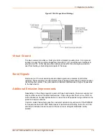
Use a multi-layer board and a separated shield layer on the solder and assembly sides of
the board, which are routed in the inner layers. (Refer to the following figure.) These
shield layers can either be connected to the RJ45s shield or to a virtual ground signal
provided by the device server.


