Principles Of Operation 61
The Secondary Microprocessor translates serial data received from the A2 board into parallel 12 bit data. The data bus is
connected directly to the four DAC/OpAmp circuits. Under control of the lip the selected DAC converts the bus data into
an analog signal. The DAC reference circuit (U503, U504) provides a +10V reference for the CV and CC DACs and a
-11.6V reference for the readback DAC. Zener VR501 provides a-6.2V reference for the OV Shunt DAC.
The CV DAC/OpAmp (U510, U513) converts the programmed voltage value from the bus or front panel into the CVPROG
signal. CVPROG is sent to the CV Error Amp and compared with the VMON signal to control the magnitude of the output
voltage in the CV mode. The range of CVPROG is 0 volts to -10 volts, which corresponds to the zero-to-full-scale output
voltage range of the supply.
The CC DAC/OpAmp (U511, U514) converts the programmed current value from the bus or front panel into the CCPROG
signal. CCPROG is sent to the CC Error Amp and is compared with the IMON signal to control the magnitude of the output
current in the CC mode. The range of CCPROG is 0 volts to -10 volts, which corresponds to the zero-to-full-scale output
current range of the supply.
The Readback Comparators (U516, U517) operate with the Readback DAC/OpAmp (U512, U515) to return the following
signals to the
P:
The monitored output voltage (VMON).
The monitored output current (IMON).
The ambient temperature (AMB_SENSE).
The programmed voltage value (CVPROG).
The programmed current value (CCPROG).
The fan detector (FAN_DEW).
The readback DAC circuit is controlled by the
P to successively approximate (to 12-bit resolution) the value of each
signal monitored. The CVPROG and CCPROG signals are used during selftest to check DAC/OpAmp operation. The
P
monitors the fan speed and ambient temperature and generates the FAN_PWM control signal to adjust fan speed depending
upon the ambient temperature measured internally in the power supply.
A dual DAC, Shunt-Trim/OV, Amplifier circuit (U520, U521) performs two functions. One is to convert the programmed
overvoltage value from the bus or front panel into the OVREF signal. The OVREF signal is compared by U502 with the
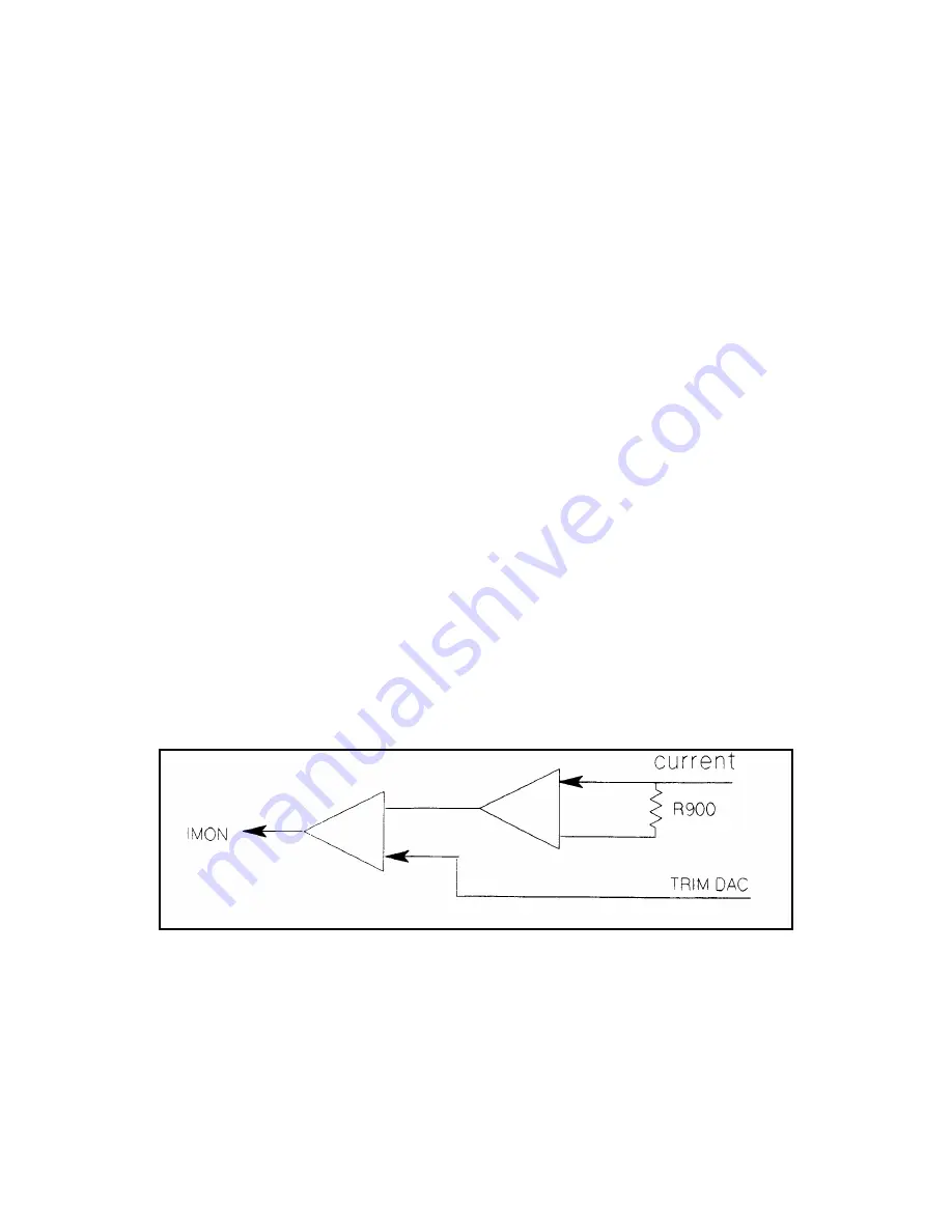
output voltage. Second, the Shunt Trim DAC calibrates the IMON signal by sampling the current flowing through
current-sense resistor (R900) on the output power bus together with the TRIM input signal.
Figure 4-1. AC Calibration of IMON
During power initiation, the secondary processor generates PWM DISABLE to the power supply's output off for 10
seconds. After 10 seconds PWM DISABLE is removed and the supply's output can be programmed.
CV/CC Control (P/O A10 Board) These circuits are shown in detail on the A10 Control Board schematic and include the
CV (constant voltage) and CC (constant current) control loops. The power supply must act as either a CV or CC supply for
any value of load impedance. Switching between CV and CC is done automatically by the CV/CC control circuits at a
value of load impedance equal to the ratio of the programmed voltage value to the programmed current value.
Содержание 669 A Series
Страница 2: ...Service Manual Keysight Series 669xA GPIB DC Power Supplies ...
Страница 3: ......
Страница 27: ......
Страница 56: ...Troubleshooting 53 Figure 3 15 3 Inch Front Panel Frame Assembly ...
Страница 57: ...54 Troubleshooting Figure 3 16 Assembly A10 Exploded View ...
Страница 58: ...Troubleshooting 55 Figure 3 17 Assembly A10 Exploded View 6690A ...
Страница 59: ...56 Troubleshooting Figure 3 18 Assembly A10 Exploded View 6691A 6692A ...
Страница 60: ...Troubleshooting 57 Figure 3 19 Three Phase Line Choke Subchassis Wiring ...
Страница 61: ...58 Troubleshooting Figure 3 20 24 Volt Fan Transformer ...
Страница 77: ...74 Diagrams Figure 6 1 Test Point Waveforms for Table 6 3 sheet 2 of 2 ...
Страница 79: ...Figure 6 3 A1 Front Panel Board Assembly Diagram ...
Страница 81: ...Figure 6 5 A2 GPIB Board Component Location ...
Страница 83: ...Figure 6 7 A3 FET Board Component and Test Point Location ...
Страница 87: ...Figure 6 11 A4 AC Input Board Component and Test Point Location 12 9 10 11 ...
Страница 89: ...Figure 6 13 A5 DC Rail Board Component and Test Point Location 13 14 ...
Страница 91: ...Figure 6 15 A6 Bias Board Component and Test Point Location 15 16 17 18 19 19 20 22 ...
Страница 94: ...Figure 6 17 Power Mesh Schematic Diagram All Models ...
Страница 103: ......


