


NXR-700
8
CIRCUIT DESCRIPTION
1. Outline
The NXR-700 is a VHF repeater operating in the 136~
154MHz frequency range.
2. Transmitter unit
The transmitter unit (X56-311 A/3) consists of the follow-
ing circuit.
(1) Internal/external reference circuit
(2) Transmitter reference 19.2MHz PLL circuit
(3) Transmitter Modulation 19.2MHz PLL circuit
(4) Transmitter DDS circuit
(5) Transmitter main PLL circuit
(6) Driver circuit
(7) Modulation level adjustment circuit
(8) AVR circuit
(9) Other circuits
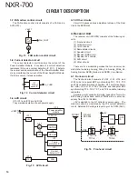
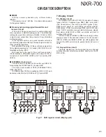
2-1. Internal/external reference circuit
The internal/external reference circuit automatically
switches signals used as reference signals among the
5.99MHz internal DDS, the 10MHz external reference signal
and the 10MHz OCXO unit.
If no OCXO unit is installed, and there is no external ref-
erence signal, the 5.99MHz internal DDS (IC601) is selected
as the reference signal.
If the OCXO unit is installed and there is no external
reference signal, the 10MHz OCXO unit is selected as the
reference signal.
If an external reference signal (CN408/ 10MHz/ 0dBm
or higher/ Zin=50
) is input, the external reference signal is
selected as the reference signal irrespective of an existing
OCXO unit.
The internal/external reference circuit consists of Q419,
Q418, D401, D403, D404, D410, D411, Q430, Q422, D601
and D607.
The DDS circuit consists of X601, IC602, IC601, Q606,
CF601, Q603, D602 and D608.
If either the OCXO 10MHz or external reference 10MHz
is selected as the reference signal, the reference output ter-
minal outputs the reference signal (CN403/ 10MHz/ +9dBm/
Zout=50
). This circuit consists of Q431, Q420 and Q425.
SW
OSC
X601
BUFF
IC602
BUFF
IC407
PLL IC
IC404
BPF
CF601
DDS
IC601
Q606
LPF
LPF
LPF
LPF
Q603
Q422
Q430
LPF
Q425
Q420
Q431
Q41
9
D601
D602
D607
D608
SW
D404
D405
D410
D411
CN403
REF_OUT
CN408
REF_IN
CN407
OCXO
TX UNIT
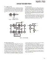
2-2. Transmitter reference 19.2MHz PLL circuit
The transmitter reference 19.2MHz PLL circuit produces
a reference frequency signal for the transmitter modulation
19.2MHz PLL circuit and the Receiver unit (X55-309) Re-
ceiver DDS circuit.
This circuit consists of Q401, Q412, Q415, Q416, Q417,
X401, IC401, IC404, and IC407.
The 5.99MHz or 10MHz signal produced by the internal/
external reference circuit is amplifi ed by IC407 and supplied
to the PLL IC (IC404) reference signal pin.
The VCXO (X401) signal enters buffer amp Q417 and is
amplifi ed by Q415. The higher harmonic wave is attenuated
by LPF and returns to IC404. Its phase is compared with
that of the reference frequency 10kHz.
The phase difference signal produced by the comparing
phase is converted to a DC voltage by a lag-lead type loop
fi lter. This DC voltage is input to the X401 control voltage
terminal for controlling the VCXO oscillating frequency.
The DC voltage passes through the IC401 operational
amplifier, and is output as a voltage signal (CVT-REF) for
monitoring the reference 19.2MHz PLL circuit lock voltage.
The stabilized 19.2MHz reference oscillating signal en-
ters the Q417 buffer amplifi er and is amplifi ed by Q412 and
Q416. The higher harmonic wave is attenuated by LPF, fed
to IC302 and used as the reference frequency signal for the
transmitter modulation 19.2MHz PLL circuit.
The 19.2MHz reference oscillating signal is also used as
the reference signal for the receiver unit (X55-309).
It enters the Q417 buffer amplifier for the receiver unit
(X55-309) and is amplifi ed by Q401. The higher harmonic
wave is attenuated by LPF and is output from CN406.
Fig. 1 Internal/external reference circuit
Содержание NEXEDGE NXR-700
Страница 110: ...NXR 700 110 MEMO ...
Страница 119: ...NXR 700 117 MEMO ...
Страница 137: ...NXR 700 135 MEMO ...
Страница 138: ...NXR 700 136 MEMO ...
Страница 140: ...NXR 700 ...
Страница 171: ...1 E CN300 RX_IF_VN ...


