


NXR-700
10
TX Mod
1
9
.2MHz
PLL circuit
IC307
5V #2
5V #1
1
9
.2MHz
Q211
CF201
5V #1
4.5MHz
Q212
5V #1
Q213
5V #1
TX main
PLL circuit
4.5MHz
IC202
DDS IC
ATT
ATT
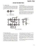
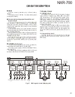
Fig. 4 Transmitter DDS circuit
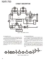
2-5. Transmitter main PLL circuit
The transmitter main PLL circuit consists of the VCO
(Q102 and Q103), PLL IC (IC101) and divide-by-2 circuit
(IC811) and produces the transmitter frequency signal.
The VCO Q102 produces transmitter frequencies from
136.000MHz to 144.995MHz. (The transmitter frequency of
the VCO is from 272.000MHz to 289.990MHz.)
The VCO Q103 produces transmitter frequencies from
145.000MHz to 154.000MHz. (The transmitter frequency of
the VCO is from 290.000MHz to 308.000MHz.)
The signal produced by the VCO (Q102 or Q103) is fed
to the buffer amplifi er and is amplifi ed by Q106. The higher
harmonic wave is attenuated by LPF and returns to the PLL
IC (IC101).
IC101 divides the VCO oscillating frequency signal and
transmitter PLL reference signal (4.5MHz), and compares
the phase with the 100kHz comparison frequency.
The phase difference signal produced by the comparing
phase is converted to a DC voltage by a lag-lead type loop
fi lter.
The DC signal is applied to varicaps D101, D102, D107,
and D108 to lock the VCO oscillator frequency with the de-
sired oscillator frequency.
At the same time, the DC signal passes through the
IC102 operational amplifier for monitoring the transmitter
main PLL lock voltage.
The output from the VCO passes through the buffer am-
plifi er Q104. The divide-by-2 circuit (IC811) divides the fre-
quency and produces the transmitter frequency. The output
level of IC811 is about +6dBm (4mW).
Q106
TX DDS
circuit
1/R
1/N
PD
Fref.=4.5MHz
R=45
Fpd=100kHz
5V #2
Q104
Q102
9
V’
9
V’
3V
5V #2
5V #2
272~
28
9
.
99
MHz
272~
308MHz
IC102
OP-AMP
IC811
4
9
6
4.5MHz
IC101
PLL IC
CVT
Driver
circuit
136~
154MHz
D108
D107
D101
Q103
9
V’
2
9
0~
308MHz
D102
1/2
ATT
ATT
Fig. 5 Transmitter main PLL circuit
2-4. Transmitter DDS circuit
The transmitter DDS circuit produces the transmitter
main PLL reference frequency signal 4.5MHz.
This circuit consists of IC307, IC202, CF201, Q210,
Q211, Q212 and Q213.
The 19.2MHz signal from the transmitter modulation
19.2MHz PLL circuit is amplifi ed by IC307 and supplied to
the IC202 reference signal pin.
IC202 produces the transmitter main PLL 4.5MHz refer-
ence frequency signal based on 19.2MHz on signal.
The spurious output by IC202 is attenuated by CF201
and LPF, 4.5MHz reference frequency signal is amplifi ed by
Q211, Q212, and Q213, and fed to the transmitter main PLL.
The comparison frequency of the transmitter main PLL is
100kHz and the PLL frequency step is 100kHz.
However, minute frequency step such as 2.5kHz and
3.125kHz because the DDS output frequency is variable.
CIRCUIT DESCRIPTION
Содержание NEXEDGE NXR-700
Страница 110: ...NXR 700 110 MEMO ...
Страница 119: ...NXR 700 117 MEMO ...
Страница 137: ...NXR 700 135 MEMO ...
Страница 138: ...NXR 700 136 MEMO ...
Страница 140: ...NXR 700 ...
Страница 171: ...1 E CN300 RX_IF_VN ...


