


NXR-700
11
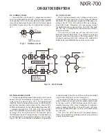
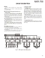
2-6. Driver circuit
The driver circuit amplifi es the transmitter frequency sig-
nal to the level required for input to the Final Unit (X45-385
A/5).
This circuit consists of RF amplifiers Q202 and Q203,
switches Q204, and Q205, and operating amplifi er IC201.
DC switches Q204, and Q205 turns the power supply
voltage of RF amplifi ers Q202, and Q203 on and off.
The output of the divide-by-2 IC (IC811) is attenuated by
attenuators R209, R210 and R211, by approximately 10dB.
So, the transmitter signal input level to Q202 is approximate-
ly –4dBm (0.4mW).
Q202 amplifi es it by approximately 15dB. So, the output
level is approxi11dBm (12.6mW).
The output from Q202 is attenuated by attenuators R217,
R218 and R219, by approximately 3dB, and amplified by
Q203 approximately by 12dB. So, the output from Q203 is
approxi20dBm (100mW). This output level is output
from the driver output connector CN802 and connected to
the Final Unit (X45-385 A/5).
Q203 has an AGC (Auto Gain Control) circuit. D201 rec-
tifi es a part of the Q203 output and converts it into DC volt-
age. It is compared with the control voltage (D_PC) by the
operation amplifi er IC201. The Q203 Gate terminal voltage
is controlled for the stabilizing Q203 output (+20dBm).
Q202
Q203
TX main
PLL circuit
8V #1
Final
unit
D201
ATT
SW
ATT
136~
154MHz
D_PC
IC201
(A/2)
IC201
(B/2)
8V #1’
CN802
136~154MHz
+20dBm
8V #1’
Q204, 205
Fig. 6 Driver circuit
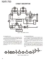
2-7. Modulation level adjustment circuit
The level adjustment circuit adjusts the modulation signal
level to provide the required level of modulation. This circuit
consists of IC301, IC304, IC305, and IC308.
The audio signal comes from the Control Unit (X53-413)
through pin 4. The modulating signal is input to IC304 from
this.
IC304 is an electronic volume control IC.
The modulation waveform balance adjustment, maximum
AF Dev. change, and adjustment are performed according
to data from the MPU using the FPU.
The modulation signal is produced by the modulating
low-pitched tone to the transmitter modulation 19.2MHz PLL
circuit and adds the high-pitched modulation to the transmit-
ter main PLL.
IC305 is an inverting amplifi er (B/2) for inverting the am-
plifi cation (A/2) of the modulating signal and synthesizing the
VCXO (X301) control voltage and modulating signal.
IC301 is a reference voltage generator (A/2) in modulat-
ing level adjusting circuit and non-inverting amplifi cation of
modulating signal with a cutoff signal of approximately 9kHz
(B/2).
Fig. 7 Modulation level adjustment circuit
CIRCUIT DESCRIPTION
Control
unit
TX Mod 1
9
.2MHz
PLL circuit
VCXO_CV
TX main
PLL circuit
VCO_MOD
Mod
signal
CN804
4
1
IC304
IC308 (B/2)
5V #2
IC301
(B/2)
5V #2
IC305
(A/2)
IC305
(B/2)
5V #2
5V #2
5V #2
TX Mod 1
9
.2MHz
PLL CP
3
2
10
4
Содержание NEXEDGE NXR-700
Страница 110: ...NXR 700 110 MEMO ...
Страница 119: ...NXR 700 117 MEMO ...
Страница 137: ...NXR 700 135 MEMO ...
Страница 138: ...NXR 700 136 MEMO ...
Страница 140: ...NXR 700 ...
Страница 171: ...1 E CN300 RX_IF_VN ...


