1-23
RC-BZ5LB/BZ5RD
RC-BZ6BU
35
36
34
33
32
31
30
29
28
27
26
25
24
23
22
21
20
19
18
17
16
15
14
13
12
11
10
9
8
7
6
5
4
3
2
1
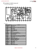
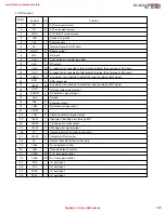
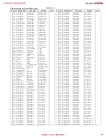
3. Pin function
PDAC
FBAL
TBAL
PDFR
PDER
PDE
PDBD
TEBPF
VDET
CROSS
TEOUT
TE-
FEOUT
FE-
/NRFDET
GND
LDOFF
VREF
ENV
OFTR
C.AGC
ARF
C.ENV
C.EA
CSBDO
BDO
CSBRT
LD
LDON
LDP
VCC
RF-
RFOUT
RFIN
PD
Pin No.
Symbol
I/O
I
O
I
--
--
I
O
I
I/O
O
I/O
I/O
I/O
O
I/O
O
O
--
O
O
I
O
I
O
O
I
O
I
I
I
I/O
I/O
I
I
I
I
I-V amp input
I-V amp input
I-V amp input
I-V amp input
E I-V amp gain control
F I-V amp gain control
Tracking balance control
Focus balance control
Inverse input pin for focus error amp
Output pin of focus error
Inverse input pin for tracking error amp
Tracking error signal output
Tracking error cross output
Input pin of tracking error through BPF
Vibration detection signal output
Reference voltage output
Function
APC amp input terminal
APC amp output terminal
APC ON/OFF control terminal
Envelope output
Ground
RF detection signal output
Of-track status signal output
BDO output pin
A capacitor is connected to this terminal to detect the envelope of RF signal
RF output
Connecting pin of AGC loop filter
RF input
RFamp output
Inverse input pin for RF amp
Power supply
Connect to ground
A capacitor is connected to this terminal to detect the envelope of RF signal
A capacitor is connected to detect the lower envelope of RF signal
A capacitor is connected to detect the lower envelope of RF signal
www.freeservicemanuals.info
11/28/2017
Digitized in Heiloo Netherlands


