background image

(No.49837)1-11

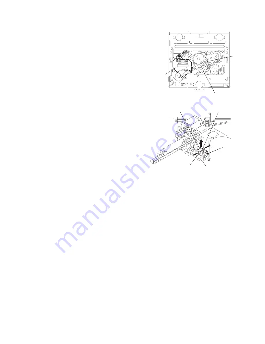
2.2.3 Removing the DET switch 

(See Figs.6 and 7)

(1) Extend the two tabs 

c

 of the feed sw. holder and pull out

the switch.

(2) Unsolder the DET switch wire if necessary.

Fig.6

Fig.7

Connector

board

DET

switch

Pickup

DET switch

Tab c

Tab c

DET switch wire

Feed sw. holder

Содержание KD-SV3000

Страница 1: ...37 2003 6 VCD CD RECEIVER 49837 2003 6 KD SV3000 TABLE OF CONTENTS 1 Precautions 1 3 2 Disassembly method 1 5 3 Adjustment 1 24 4 Description of major ICs 1 27 Area Suffix U Other Areas VIDEO CD PBC ENTER CD EQ FM AM VOL DOWN UP ATT OSD AUDIO 1 2 3 4 5 6 7 8 0 9 RETURN ...

Страница 2: ...7 5 MHz to 108 MHz AM 531 kHz to 1 602 kHz FM Tuner Usable Sensitivity 11 3 dBf 1 0 µV 75 Ω 50 dB Quieting Sensitivity 16 3 dBf 1 8 µV 75 Ω Alternate Channel Selectivity 400 kHz 65 dB Frequency Response 40 Hz to 15 000 Hz Stereo Separation 35 dB Capture Ratio 1 5 dB AM Tuner Sensitivity 20 µV Selectivity 35 dB CD PLAYER SECTION Type Compact disc player Signal Detection System Non contact optical p...

Страница 3: ... formed during molding may be left over on some parts of the chassis Therefore pay attention to such burrs in the case of preforming repair of this system Please use enough caution not to see the beam directly or touch it in case of an adjustment or operation check ...

Страница 4: ...in the optical pickup The tester s internal power source can easily destroy the laser diode 1 3 Handling the traverse unit optical pickup 1 Do not subject the traverse unit optical pickup to strong shocks as it is a sensitive complex unit 2 Cut off the shorted part of the flexible cable using nippers etc after replacing the optical pickup For specific details refer to the replacement procedure in ...

Страница 5: ...ck side of the main body then remove the bottom cover from the main body CAUTION When releasing the joints using a screwdriver do not damage the main board Fig 2 2 1 3 Removing the front chassis assembly See Fig 3 Prior to performing the following procedures remove the front panel assembly and bottom cover 1 Remove the screw A on the both sides of the main body 2 Release the two joints d and two j...

Страница 6: ...screws F at taching the rear bracket on the back side of the main body 2 Remove the rear bracket Reference During reassembly before fixing the rear bracket onto the main body insert the video out cable into the slot Fig 5 2 1 6 Removing the main board See Fig 6 Prior to performing the following procedure remove the front panel assembly front chassis assembly heat sink bottom cover and rear bracket...

Страница 7: ...D CD mechanism board 3 Move the VCD CD mechanism board in the direction of the arrow to release it from the joint f Fig 7 2 1 8 Removing the CD mechanism assembly See Fig 8 Prior to performing the following procedure remove the front panel assembly front chassis assembly heat sink bottom cover rear bracket main board and VCD CD mechanism board 1 Remove the three screws J attaching the top chassis ...

Страница 8: ... panel assembly 1 Remove the four screws K on the back side of the front panel assembly See Fig 9 2 Release the thirteen joints g See Fig 10 3 Release the joint h and take out the front board See Fig 11 Fig 9 Fig 10 Fig 11 K K K Joints g Joints g Joints g Joints g Joints g Joints g Front board Joint h Front panel assembly ...

Страница 9: ...moving the top cover See Figs 1 and 2 1 Remove the four screws A on the both side of the body 2 Lift the front side of the top cover and move the top cover backward to release the two joints a Fig 1 Fig 2 A A A Joints a Top cover Joints a Top cover ...

Страница 10: ...nector board 2 Solder the short circuit point on the pickup 3 Disconnect the flexible wire from the pickup 4 Move the connector board in the direction of the arrow to release the two joints b 5 Unsolder the wires on the connector board if necessary CAUTION Unsolder the short circuit point after reassembling Fig 3 Fig 4 Fig 5 B Connector board Pickup Short circuit point Joints b Wires Pickup Short ...

Страница 11: ... switch See Figs 6 and 7 1 Extend the two tabs c of the feed sw holder and pull out the switch 2 Unsolder the DET switch wire if necessary Fig 6 Fig 7 Connector board DET switch Pickup DET switch Tab c Tab c DET switch wire Feed sw holder ...

Страница 12: ...he chassis unit to the frame CAUTION The shape of the suspension spring L and R are dif ferent Handle them with care When reassembling make sure that the three shafts on the underside of the chassis unit are inserted to the dampers certainly Fig 8 Fig 9 Suspension spring L Suspension spring L Suspension spring R Suspension spring R Chassis unit Frame Chassis unit Frame Shafts Shaft Damper Damper D...

Страница 13: ...cedure remove the top cover 1 Remove the clamper arm spring 2 Move the clamper assembly in the direction of the arrow to release the two joints d Fig 10 Fig 11 Clamper arm spring Chassis rivet assembly Joint d Joint d Clamper assembly Clamper arm spring Clamper assembly Joint d Joint d Chassis rivet assembly ...

Страница 14: ...e the screw C and move the loading feed motor as sembly in the direction of the arrow to remove it from the chassis rivet assembly 2 Disconnect the wire from the loading feed motor assembly if necessary CAUTION When reassembling connect the wire from the loading feed motor assembly to the flame as shown in Fig 12 Fig 12 Fig 13 Loading feed motor assembly Loading feed motor assembly C ...

Страница 15: ... F 2 Reattach the feed sw holder to the feed rack while setting the joint g to the slot of the feed rack and setting the joint f of the feed rack to the switch of the feed sw holder correct ly 3 As the feed sw holder is temporarily attached to the pickup unit set to the gear of the joint g and to the bending part of the chassis joint h at a time CAUTION Make sure that the part i on the underside o...

Страница 16: ...e slot of the chassis rivet assembly respectively and join the joint k at a time Fig 19 Fig 20 2 2 10 Removing the top plate assembly See Fig 21 Prior to performing the following procedure remove the top cover connector board chassis unit and clamper assembly 1 Remove the screw H 2 Move the top plate assembly in the direction of the arrow to release the two joints r 3 Unsolder the wire marked s if...

Страница 17: ...irection of the arrow to release the joint u 2 Unsolder the wire of the mode sw marked s if necessary 3 Turn the select lock arm in the direction of the arrow to re lease the two joints v 4 The select lock arm spring comes off the select lock arm at the same time Fig 22 Fig 23 Mode sw Select lock arm Joint t Link plate Joint u s Top plate Top plate Select lock arm Select lock arm spring Select loc...

Страница 18: ... the underside of the select lock arm and join the select lock arm to the slots joint v Turn the select lock arm as shown in the figure 3 Reattach the mode sw while setting the part t to the first peak of the link plate gear and join the joint u CAUTION When reattaching the mode sw check if the points y and z are correctly fitted and if each part operates properly Fig 24 Fig 25 Fig 26 Select lock ...

Страница 19: ... 29 and 30 REFERENCE Reverse the above removing procedure 1 Reattach the link plate spring 2 Reattach the link plate to the link plate spring while joining them at joint d 3 Reattach the joint a of the select arm R to the first peak of the link plate while joining the two joints b with the slots Then turn the select arm R as shown in the figure The top plate is joined to the joint c CAUTION When r...

Страница 20: ... 5 Extend the lock arm rivet assembly outward and release the joint j from the boss of the chassis rivet assembly The roller guide springs on both sides come off at the same time CAUTION When reassembling reattach the left and right roller guide springs to the lock arm rivet assembly before reat taching the lock arm rivet assembly to the chassis rivet assembly Make sure to fit the part k of the ro...

Страница 21: ...chassis unit pickup unit and top plate assembly 1 Remove the screw K attaching the loading gear bracket The loading gear 6 and 7 come off the loading gear brack et 2 Pull out the loading gear 5 Fig 35 Fig 36 K Loading gear bracket Loading gear 6 Loading gear 5 Loading gear 3 K Loading gear bracket Loading gear 6 Loading gear 5 Loading gear 7 ...

Страница 22: ...Remove the loading gear 1 8 Move the change plate rivet assembly in the direction of the arrow to release from the three shafts of the chassis rivet assembly upward See Fig 38 9 Detach the loading gear plate rivet assembly from the shaft of the chassis rivet assembly upward while releasing the joint p See Figs 38 and 40 10 Pull out the loading gear 4 Fig 37 Fig 38 Fig 39 Fig 40 Slot m Slot m Joint...

Страница 23: ...ng procedure remove the top cover connector board chassis unit and clamper assembly 1 Remove the two screws L attaching the spindle motor as sembly through the slot of the turn table on top of the body 2 Unsolder the wire on the connector board if necessary Fig 41 Fig 42 L Turn table L Turn table Spindle motor ...

Страница 24: ... there is a loss of 6dB between SSG output and antenna input The loss of 6dB need not be considered since direct reading of figures are applied in this working standard How to connect the extension cable for adjusting Caution Be sure to attach the heat sink and rear bracket onto the power amplifier IC and regulator IC respectively before supply the power If voltage is applied without attaching the...

Страница 25: ... software version Press the F SKIP key VCD 144 SUB 144 is indicated on the LCD VCD CD control IC software version Press the F SKIP key Press the F SKIP key Sequence of LCD diaplay Press the B SKIP MAIN VCD CD SUB MAIN Press the F SKIP MAIN SUB VCD CD MAIN Cancellation of service mode No operation for ten seconds Return to normal display Press the key except for F SKIP or B SKIP key Return to norma...

Страница 26: ...tical block do not touch the semi fixed resistor If the laser power is lower than the specified value the la ser diode is almost worn out and the laser pickup should be replaced If the semi fixed resistor is adjusted while the pickup is functioning normally the laser pickup may be damaged due to excessive current 3 4 Replacement of laser pickup Is RF output 1 3 0 4Vp p Replace it NO YES O K Turn o...

Страница 27: ... VCC GND VPP A0 A17 ADDRESS INPUTS OE CE PGM X DECODER Y DECODER OUTPUT BUFFERS Y GATING DATA OUTPUTS O0 O7 CELL MATRIX IDENTIFICATION Pin No Symbol Function 1 VPP Power supply 2 A16 Address input 3 A15 Address input 4 A12 Address input 5 to 12 A7 to A0 Address inputs 13 to 15 O0 to O2 Outputs 16 O3 to O7 Outputs 17 to 21 GND Ground 22 CE Chip enable 23 A10 Address input 24 OE Output enable 25 A11...

Страница 28: ...mable for rising or falling edge 41 HSYNC I O Horizontal sync programmable for rising or falling edge 42 CPUCLK I RISC and system clock input 43 PCLK2X I O Doubled pixel clock I O for screen video interface 44 PCLK I O 27 MHz pixel clock qualifier I O for screen video interface 45 49 AUX 0 7 I O Auxillary control AUX0 and AUX1 are open collectors 50 VSS I Ground 51 VDD I 2 85V power supply 52 54 A...

Страница 29: ... lock loop PLL clock frequency of CPUCLK pin 42 00 bypass PLL 01 54MHz PLL 10 67 5MHz PLL 11 81MHz PLL 90 ATCLK I O Audio transmit bit clock 91 ATFS O Audio interface transmit frame sync SEL_PLL1 I Used with SEL_PLL0 pin 89 to select phase lock loop PLL clock frequency of CPUCLK pin 42 92 MA9 O Multiplexed memory row and column address DOE O Memory output enable active low 93 AIN I Audio interface...

Страница 30: ... C2PO or Interrupt input or Control Pin 38 AUX13 I O Serial Interrupt CD Mute or Control Pin 39 AUX14 I O Servo SCOR S0S1 or Interrupt Input or Control Pin 40 AUX15 I O Interrupt Input or Control Pin 81 83 85 93 95 97 99 8 DSC_D 7 0 I O Data for programming to access Internal registers 10 DSC_S I Strobe for programming to access Internal registers 12 DCLK O Dual purpose pin DCLK is the MPEG decode...

Страница 31: ...rolytic in parallel with 0 1µF 43 VREFP I DAC and ADC maximum reference Bypass to VCMR with 10µF in parallel with 0 1µF 44 VCCAA I Analog VCC 5V 45 46 AOR AOR O Right channel output 47 48 AOL AOL O Left channel input 49 MIC1 I Microphone input 1 50 MIC2 I Microphone 2 52 VREF I Internal resistor divider generates Common Mode Reference CMR voltage Bypass to analog ground with 0 1µF 53 VREFM I DAC a...

Страница 32: ...al for AGC loop filter capacitor 8 ARF O AGC output terminal 9 CEA I Capacitor connecting terminal for HPF Amp 10 3TOUT O 3 TENV output terminal 11 CBDO I Capacitor connecting terminal for envelope detection on the darkness side 12 BDO O BDO output terminal 13 COFTR I Capacitor connecting terminal for envelope detection on the light side 14 OFTR O OFTR output terminal 15 NRFDET O NRFDET output ter...

Страница 33: ... RAS Row address strobe UCAS Columu address strobe upperbyte control LCAS Columu address strobe lower byte control WE Write enable OE Output enable DQ1 DQ16 Dara inputs outputs Vcc 5V power supply Vss Ground NC No connection RAS CLOCK GENERATOR CAS CLOCK GENERATOR WE CLOCK GENERATOR OE CLOCK GENERATOR REFRESH COUNTER ADDRESS BUFFWRS AND PREDECODERS ROW DECODERS MEMORY ARRAY I O BUFFER Data I O BUS...

Страница 34: ... LA47505 IC321 Power amp Terminal layout Muting On Time Control Circuit protective circuit Mute circuit Protective circuit Ripple Filter Stand by Switch 11 16 14 13 25 15 10 4 1 12 22 17 19 18 21 23 24 2 3 5 8 7 9 20 6 ...

Страница 35: ...for front Rch 6 Vcc1 2 Power input 7 OUTRR Output for rear Rch 8 GND2 Power GND 9 OUTRR Output for rear Rch 10 VREF Ripple filter 11 INRR Rear Rch input 12 INFR Front Rch input 13 SGND Signal GND 14 INFL Front Lch input 15 INRL Rear Lch input 16 ONTIME Power on time control 17 OUTRL Output for rear Lch 18 GND3 Power GND 19 OUTRL Output for rear Lch 20 Vcc3 4 Power input 21 OUTFL Output for front 2...

Страница 36: ... B VIN1 B S GND VIN1 SW MUTE VREF_IN FR VCC_S REG OUT REG_IN VIN2G VIN2 VIN3G VIN3 28 27 26 25 24 23 22 FR 21 20 19 18 17 16 15 Level shift Level shift H L VIN1_SW 33k 11k 33k 33k 11k 11k Signal system GND Power system GND Power system GND Signal system power supply 5VREG PNPTr External It is ON OFF as for all outputs H ON L OFF H OP AMP_A L OP AMP_B MUTE Level shift Level shift 33k 11k ...

Страница 37: ...inal 11 VO4 CH4 Output terminal 12 VCCP2 CH3 and CH4 power steps power supply 13 VIN4 CH4 Input terminal 14 VIN4G CH4 Input terminal For gain adjustment 15 VIN3 CH3 Input terminal 16 VIN3G CH3 Input terminal For gain adjustment 17 VIN2 CH2 Input terminal 18 VIN2G CH2 Input terminal For gain adjustment 19 REGIN External PNP transistor base connection 20 REG OUT 5VREG output terminal and external PN...

Страница 38: ... H ANT output ON 8 VCC Connected to VCC 9 BATT DET Low battery detect 10 AUDIO OUT Output voltage is 9V when M or H level applied to CTRL pin 11 CTRL L BIAS OFF M BIAS ON H CD ON 12 CD OUT Output voltage is 8V when H level applied to CTRL pin 13 ILM AJ Adjustment pin for ILM output voltage 14 ILM OUT Output voltage is 10V when M or H level applied to CTRL pin 15 GND Connected to GND 2 1 11 12 10 1...

Страница 39: ... NC Not connect 23 UDSASTB I O ES3883 STB for uDSA 24 UDSADAT I O ES3883 DAT for uDSA 25 UDSAACK I O ES3883 ACK for uDSA 26 NC Not connect 27 BLKCK I SubQ blk clk 28 GND Ground 29 PS2 I PS2 30 31 GND Ground 32 DSASTB I O ES3880 STB for DSA 33 DSADAT I O ES3880 DAT for DSA 34 DSAACK I O ES3880 ACK for DSA 35 PS1 I O PS1 slave 36 to 48 NC Not connect 49 REST I O Rest SW 50 LM O Loading motor control...

Страница 40: ... VCO AVDD2 SUB CODE BUFFER SSEL SQCK SUBQ AVDD2 CLVS CRC BLKCK CLDCK SBCK SUBC DEMPH RESY FLAG6 RESY EFM DEMODULATION SUBCODE DEMODULATION SYNC INTERPOLATION 16k SRAM CIRC ERROR CORRECTION DEINTERLEVE LRCKIN MSEL BCLK SSEL SRDATAIN PSEL IOSEL DIGITAL DEEMPHSIS 8TIMES OVER SAMPUNC DIGITAL FILTER 1BIT DAC LOGIC S PEM R PEM L DIGITAL AUDIO INTERFASE DIGITAL AUDIO INTERFASE INTER POLATION SOFT MUTING ...

Страница 41: ...ignal input Analog input 33 TE I Tracking error signal input Analog input 34 RF ENV I RF envelope signal input Analog input 35 VDET I Vibration detect signal input H detect 36 OFT I Off track signal input H off track 37 TRCRS I Track cross signal input 38 RFDET I RF detect signal input L detect 39 BDO I BDO input pin L detect 40 LDON O Laser ON signal output H on 41 PLLF2 Not used 42 TOFS O Tracki...

Страница 42: ...t Block diagram 4 17 RT9161 A 27CG X IC105 Regulator Pin layout Block diagram Pin function 1 2 3 1 INPUT 2 GND 3 OUTPUT INPUT OUTPUT GND 1 2 3 GND VIN TAB VOUT VIN GND VOUT Error Amp 1 2V Reference Pin Name Function VOUT Output Voltage GND Ground VIN Power Input ...

Страница 43: ...e Display is forcibly turned OFF SG1 to SG52 COM1 to COM3 are set to LOW See Note 1 When this pin is set to High the Displa is ON 58 VDD1 I Used for the 2 3 Bias Voltage when the Bias Voltages are provied externally Connect to VDD2 when 1 2 Bias is used 59 VDD2 I Used for 1 3 Bias Voltage when the Bias Voltages are provided externally Connect to VDD1 when 1 2 Bias is used 60 VSS Ground Pin 61 OSC ...

Страница 44: ... A D input 31 SM I S meter electric field strength input 32 AVSS Ground for A D converter Connect to ground 33 REGCPU Regulator for CPU power supply 34 VDD Power supply 35 REGOSC Power supply for oscillator circuit 36 XOUT O Crystal oscillator connect terminal for system clock 37 XIN I Crystal oscillator connect terminal for system clock 38 GND Connect to ground 39 IFCCONT O IFC output prohibition...

Страница 45: ...ert detection on power OFF 79 P SAVE1 I Power save 1 ACC detection L Power save 80 P SAVE2 I Power save 2 BATTERY detection L Power save 81 P SAVE SLAVE O Power save 1 control signal output to mecha micon 82 GND Connect to ground 83 to 91 NC Not connect 92 MUTE O Mute control signal output 93 TEL MUTING I Tel muting input 94 POWER CONT O Power supply IC control signal output 95 to 97 NC Not connec...

Страница 46: ...front 5 TL I Treble control capacitor left channel or input from an external equalizer 6 B2L Bass control capacitor left channel or output to an external equalizer 7 B1L Bass control capacitor left channel 8 IVL I Input volume 1 left control part 9 ILL I Input loudness left control part 10 QSL O Output source selector left channel 11 IDL Not used 12 MUTE Not used 13 ICL I Input C left source 14 IM...

Страница 47: ... No 49837 1 47 ...

Страница 48: ... No 49837 AV MULTIMEDIA COMPANY MOBILE ENTERTAINMENT CATEGORY 10 1 1chome Ohwatari machi Maebashi city 371 8543 Japan VICTOR COMPANY OF JAPAN LIMITED WPC Printed in Japan ...

Отзывы: