background image

12

0.5 Form Factor

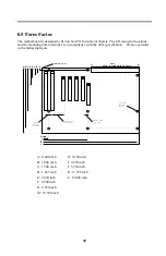
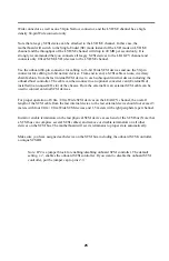
The motherboard is designed to fit into an ATX form-factor chassis. The I/O connector locations
and the mounting hole locations are in compliance with the ATX specification.  Please see detail
in the following figure.

Datum (0, 0)

A

B

C

D

E

F

G

H

I

J

K

              6.250
R E A R   I / O   W I N D O W   I N   C H A S S I S

M

0.156 inch
Mounting
Holes

L

0.800 TYP.
Between
Connectors

1.612 Pin 1 ISA
 to Pin 1 PCI

0.768 Pin 1 AGP
 to Pin 1 PCI

A: 0.400 inch

H: 0.150 inch

B: 1.000 inch

I: 0.650 inch

C: 1.300 inch

J: 5.550 inch

D: 1.625 inch

K: 11.750 inch

E: 2.630 inch

L: 12.000 inch

F: 6.500 inch

G: 9.350 inch

M: 10.390 inch

Содержание DGL200

Страница 1: ...t of Directive 89 336 ECC for Electromagnetic Compatibility Compliance was demonstrated to the following specifications as listed in the official Journal of the European Communities EN 50081 1 Emissions EN 55022 Radiated Class B EN 55022 Conducted Class B EN 60555 2 Power Harmonics EN 50082 1 Immunity IEC 801 2 Electrostatic Discharge IEC 801 3 RF Radiate IEC 801 4 Fast Transient ...

Страница 2: ...law All rights are reserved No any part of this document may be used or reproduced in any forms or by any means or stored in a database or retrieval system without prior written permission from Iwill Corp This manual is subject to change without notice PMDBL1H12AE Trademark Intel Pentium are trademarks of Intel Corporation IWILL and IWILL logo are trademarks of IWILL Corp Sound Blaster is a regist...

Страница 3: ...ON 16 2 1 PREPARATION AND INSPECTION 16 2 2 UNPACK THE DGL200 16 2 3 INSTALLATION PROCEDURES 17 CHAPTER 3 27 SYSTEM BIOS SETUP 27 3 1 INTRODUCTION 27 3 2 MAIN MENU 29 3 3 STANDARD CMOS SETUP 30 3 4 BIOS FEATURES SETUP 32 3 5 CHIPSET FEATURES SETUP 37 3 6 POWER MANEGEMENT SETUP 39 3 7 PNP PCI CONFIGURATION 43 3 8 INTEGRATED PERIPHERALS 44 3 9 LOAD SETUP DEFAULTS 47 3 10 IWILL SMART SETTING 47 3 11 ...

Страница 4: ...3 12 IDE HDD AUTODETECTION 48 3 13 SAVE EXIT SETUP 48 3 14 EXIT WITHOUT SAVING 48 CHAPTER 4 49 SCSI BIOS SETUP 49 4 1 INTRODUCTION 49 4 2 CONFIGURE VIEW HOST ADAPTER SETTINGS 49 4 3 SCSI DISK UTILITIES 53 ...

Страница 5: ...ions which compares dates or uses relative dates to perform functions will see an incorrect dates Motherboards contain BIOS which is one of the key ingredients to check for systems designed to handle the year 2000 All motherboards currently shipped from Iwill contain BIOS capable of handling the year 2000 date correctly The BIOS contains a feature that checks the least two significant digits of th...

Страница 6: ...RAM or Registered DIMM 64 bit data interface with ECC support 0 1 4 SCSI Subsystem Adaptec AIC 7896 PCI Bus Master Dual Ultra2 SCSI Host Adapter Providing two LVD SE channels Providing up to 80 MB sec sustained throughput on LVD SE channel LVD devices only Providing two 68 pin connectors on LVD SE channel and one 50 pin LVD SE channel Supports maximum cable length up to 12 meters on LVD SE channel...

Страница 7: ... BIOS Using Flash ROM to provide on board upgrade ability without changing components Plug and Play compatible Supports Advanced Power Management APM Supports Creative SB LINK to deliver Sound Blaster 16 compatibility 0 2 Environment Requirements Temperature 0 55 degrees C operating or storage 5 to 95 non condensing relative humidity At least a 250 W power supply The power supply must comply with ...

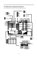
Страница 8: ...R DIMM0 3 FDC JP2 J43 IR 1 FIRRX CIRRX VCC IRRX GND IRTX NC 7 LID ON GND 5VSB 1 3 GND 12V SENSE 1 3 1 2 SCSI Enable 2 3 SCSI Disable 1 1 1 2 Normal 2 3 Clear CMOS 3 550 400 450 500 RS0 RS1 SB LINK GNT 1 5 6 2 GND REQ GND SIRQ 1 2 Disable KB ON 2 3 Enable KB ON 1 3 KB ON 1 1 ATPWR FAN1A FAN3 FAN2 2A 4 LVD SE CH A LVD SE CH B ISA Tmp1 Tmp2 3 JP11 JX2 JX1 1 10 11 20 RST ALED KL SPKR Cathode Anode Res...

Страница 9: ...ctor J34 USB Two USB connectors J35 MS PS 2 mouse connector J35 KB PS 2 keyboard connector J37 J38 PWR Standard ATX power connector J39 FAN1 Processor fan header J66 FAN1A Processor fan header J40 FAN2 Processor fan header J67 FAN2A Processor fan header J41 FAN3 System fan header J65 FAN4 System fan header J68 FAN5 System fan header J42 PWR ON Remote power on off header J43 J43 Front panel I O hea...

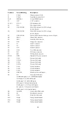
Страница 10: ...or clearing CMOS JP2 SCSI Jumper for SCSI enable disable JP3 JP3 Jumper for processor frequency selection JP5 JP5 Jumper for PCI devices compatibility JP10 JP10 Power on function for BIOS or hardware control select JP11 JP11 Chassis Intrusion JX1 JX1 SMBUS Connect JX2 JX2 Internal Modem Wake up connect ...

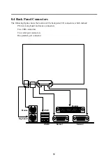
Страница 11: ...ng figure shows the location of the back panel I O connectors which include PS 2 style keyboard and mouse connectors Two USB connectors Two serial port connectors One parallel port connector Serial 1 Mouse Keyboard Parallel Serial 2 USB1 USB0 ...

Страница 12: ...lease see detail in the following figure Datum 0 0 A B C D E F G H I J K 6 250 REAR I O WINDOW IN CHASSIS M 0 156 inch Mounting Holes L 0 800 TYP Between Connectors 1 612 Pin 1 ISA to Pin 1 PCI 0 768 Pin 1 AGP to Pin 1 PCI A 0 400 inch H 0 150 inch B 1 000 inch I 0 650 inch C 1 300 inch J 5 550 inch D 1 625 inch K 11 750 inch E 2 630 inch L 12 000 inch F 6 500 inch G 9 350 inch M 10 390 inch ...

Страница 13: ... the processor frequency Simply place one jumper cap onto the speed number according to the internal frequency you see on your processor For example select 400 for a Pentium II Xeon processor 400 MHz Step 4 Install the memory module At least one piece of 168 pin 3 3V unbuffered SDRAM Registered DIMM is needed to be located into the DIMM sockets Step 5 Connect the internal peripherals The internal ...

Страница 14: ...gnal of PLED header Signal of KL header Pin 11 Anode Pin 14 KEYLOCK Pin 12 NC Pin 15 Ground Pin 13 Cathode Step 9 Connect the IDE LED The 2 pin IDE LED header is located on pins 5 6 marked as ALED of the front panel connector Connect the chassis s LED to this header Signal of ALED header Pin 5 Anode Pin 6 Cathode Step 10 Connect the SCSI LED The 2 pin SCSI LED header is located on pins 7 8 marked ...

Страница 15: ...r supply Step 14 Install the Keyboard Connect the keyboard to the PS 2 keyboard connector at the back panel Step 15 Install the Display Card Insert the display card into the ISA PCI or AGP expansion slot Step 16 Connect the External Peripherals The external device means devices outside the computer chassis like the serial mouse printer PS 2 mouse external modem etc Step 17 Power on the system Once...

Страница 16: ...in your system 2 2 Unpack the DGL200 You should find the following components when opening the box l One motherboard l One sets of Pentium II Xeon Retention kit DRM l One 34 pin floppy cable l One 40 pin IDE cable l One 50 pin Narrow SCSI cable l One Quick Installation Guide l One Iwill PowerInstaller CD diskette l One EZ SCSI Driver diskette l One LANDesk Client Management CD Optional For install...

Страница 17: ...cache thermal plate and back cover The processor connects to the motherboard through the Slot 2 connector a 330 pin edge connector When mounted in a Slot 2 connector the processor is secured by a retention mechanism attached to the motherboard First screw the main body of Slot 2 retention mechanism to the motherboard then insert the processor cartridge along the retention mechanism in vertical dir...

Страница 18: ...68 pin DIMMs with gold plated contacts 3 3 V memory module only ECC logic detects multiple bit errors and corrects single bit errors SDRAM Unbuffered SDRAM Registered DIMM 16 64 Mbit DRAM technology Symmetrical and asymmetrical DRAM addressing Single sided or double sided DIMMs Registered and Unbuffered DIMMs can NOT be installed on the same motherboard Memory can be installed in DIMM sockets with...

Страница 19: ... ZIP and LS 120 devices If two devices are connected to one channel one should be set to Master and the other one to Slave Refer to device operation guide Simply connect the 40 pin IDE cable between the IDE ATAPI devices and these connectors on the motherboard For a performance reason we suggest that connect the disk drive to the primary channel and other devices like CD ROM to the secondary chann...

Страница 20: ...l hub can be connected to either port 2 3 10 PS 2 keyboard and mouse connectors KB and MS The keyboard connector is a 6 pin mini DIN connector located on the back panel the bottom one Simply connect the standard PS 2 keyboard into this connector The PS 2 mouse connector is a 6 pin mini DIN connector on the back panel Simply connect the PS 2 mouse into this connector Note that power to the computer...

Страница 21: ... on or off At least two seconds must pass before the power supply will recognize another on off signal Note Hold the power on switch in for four seconds will force the system switch off 2 3 14 Front panel connector J43 This connector contains several headers which are connected to button or switch located on front panel of the chassis 2 3 14 1 IDE LED header ALED The 2 pin IDE LED header is locate...

Страница 22: ... Signal of PLED header Signal of KL header Pin 11 Anode Pin 14 KEYLOCK Pin 12 NC Pin 15 Ground Pin 13 Cathode 2 3 14 5 SPEAKER header SPKR The 4 pin speaker header is located on pins 17 20 marked as SPKR of the front panel connector The speaker provides error beep code information during the POST in the event that the computer can not use the video interface Signal of SPKR header Pin 17 VCC Pin 18...

Страница 23: ...the Wake on LAN technology The NIC monitors network traffic When it detects a Magic Packet it asserts a signal through the WOL header to wake up the computer This signal can wake up the computer only when the power cord is still plugged into the socket and the computer is turned off Signal of WOL header Pin 1 5VSB Pin 2 Ground Pin 3 LID_ON 2 3 18 Clear CMOS jumper block CLRTC To reset the RTC Real...

Страница 24: ...is has been opened The circuitry will then alert the user with a warning message when the system is turned on 2 3 22 SMBus connector JX1 SMBus System Management Bus connector for system transfer control signal 1 2 3 23 Internal modem Wake Up Function connector JX2 This connector for Power on by Ring function as internal modem 2 3 24 Power On function Select When 1 2 pin is ON Power On function by ...

Страница 25: ...an optional converter card External Kit installed in an unused I O slot of the chassis From the external kit an external SCSI cable can be used to connect external SCSI devices For proper operation of Ultra Ultra Wide SCSI devices on the LEAGCY channel the overall length of the SCSI cable from the last internal device to the last external device should not exceed 3 meters with four Ultra Ultra Wid...

Страница 26: ...ng figure shows the correct SCSI bus topology Ext Device Terminator 8 bit cable 16 bit cable Int Narrow Device Int Wide Device Int Wide Device Int Narrow Device Ext Device External Kit Wide Connector Narrow Connector ...

Страница 27: ...e data can be lost if a power outage occurs while the BIOS being updated in flash memory The BIOS can be recovered from a diskette To create a BIOS recovery diskette a bootable diskette must be created and the recovery files copied to it The recovery files are available from Iwill Note No video is displayed during the recovery process 3 1 3 Enter BIOS setup program The BIOS setup program is access...

Страница 28: ...by the system manufacturer to provide the absolute maximum performance and reliability It is very dangerous to change any setting without full understanding We strongly recommend that DO NOT update your BIOS if the system works perfect DO NOT change any setting unless you fully understand what it means If the system does not work smoothly after changing the BIOS setting follow the procedures descr...

Страница 29: ...dvanced features available through the BIOS CHIPSET FEATURES SETUP Specifies advanced features available through the chipset POWER MANAGEMENT SETUP Specifies power management features PNP PCI CONFIGURATION Specifies Plug and Play and PCI features INTEGRATED PERIPHERALS Specifies on board controller features LOAD SETUP DEFAULTS Load the manufacturer default setting into CMOS IWILL SMART SETTING Spe...

Страница 30: ... Options Description 1 45 Specifies pre defined disk drive type User Specifies disk drive type by user Auto BIOS automatically fills in the values for the cylinders heads and sectors fields None No disk drive attached 3 3 3 2 Cylinders If device TYPE is set to Auto this field reports the number of cylinders for your hard disk and can not be modified If the TYPE is set to User you must type the cor...

Страница 31: ...cted 3 3 5 Floppy 3 Mode Support 3 Mode floppy drive is a kind of 3 5 inches drive which is used at NEC PC98 computer It supports 1 2M and 1 44M format with the same drive This field specifies which drive 3 Mode is supported When a floppy drive is specified to support 3 Mode the respective drive setting in Drive A Drive B field will be invalid Options Description Disabled No 3 Mode drive is connec...

Страница 32: ...no options 3 3 10 Other Memory This refers to the memory located in the 640K to 1024K address space This is memory that can be used for different applications DOS uses this area to load device drivers in an effort to keep as much base memory free for application programs The BIOS is the most frequent user of this RAM area since this is where it shadows RAM This field has no options 3 4 BIOS FEATUR...

Страница 33: ...ot From LAN First This field configures the boot from the LAN first advanced section 3 4 7 Options Enabled Disabled 3 4 7 Boot Sequence This field configures the boot sequence of boot devices Options Description A C SCSI System will first try to boot from floppy drive then master IDE disk drive on primary channel and then SCSI disk drive C A SCSI Master IDE disk drive on primary channel floppy dri...

Страница 34: ...Enabled Disabled 3 4 9 Boot Up Floppy Seek When enabled BIOS will check floppy drive status during POST If an error occurred system will be paused and an error message will be prompted Options Enabled Disabled 3 4 10 Hard Disk Write Protect This field configures Hard Disk write protect Options Description Enabled Hard Disk write protect Disabled Hard Disk can be accessed read and write both 3 4 11...

Страница 35: ... Msec fields will be available Options Enabled Disabled 3 4 15 Typematic Rate Chars Sec This field specifies how many characters will be prompted in one second when a key is pressed continuously Options 6 8 10 12 15 20 24 30 3 4 16 Typematic Delay Msec This field specifies the delay between when a key was first pressed and when the acceleration begins Options 250 msec 500 msec 750 msec 1000 msec 3...

Страница 36: ...hen enabled the video BIOS will be copied to system memory and increase the video speed Options Enabled Disabled 3 4 22 C8000 CBFFF CC000 CFFFF D0000 D3FFF Shadow D4000 D7FFF D8000 DBFFF DC000 DFFFF Shadow When enabled the extended ROM data located at the respective address range will be copied to system memory Options Enabled Disabled 3 4 23 OS Select for DRAM 64MB When enabled this field allows ...

Страница 37: ...uter Options 2 3 3 5 3 SDRAM CAS latency TIME You con select CAS latency time in HCLKs of 2 or 3 The system board designer should set the values in this field depending on the DRAM installed Options 2 3 3 5 4 SDRAM Precharge Control This field specifies the length of the RAS part of the DRAM system memory access cycle when Synchronous DRAM system memory is installed in the computer Options Enabled...

Страница 38: ...ss range Any host cycles that match this memory hole are passed on to the add in cards Options Enabled Disabled 3 5 12 Passive Release When enabled the south bridge PIIX4 will support the Passive Release mechanism when it is a PCI master The PCI revision 2 1 compliant requires this field to be enabled This field is for experienced users only Options Enabled Disabled 3 5 13 Delayed Transaction When...

Страница 39: ...ach power saving mode has a respective timer The value of the timer can be assigned or reloaded and it will count down to zero When the timer equals to zero the system will be forced into the related power saving mode If any predefined signal or event is detected during the timer counting period the timer will be reloaded automatically 3 6 1 ACPI Function This item allows you to enable disable the...

Страница 40: ...e power saving mode which will shut off the video Options Doze Standby Suspend NA 3 6 6 Doze Mode This field specifies the timer value of Doze Mode It is available only when the Power Management field set to User Define Options 1 Min 2 Min 4 Min 8 Min 12 Min 20 Min 30 Min 40 Min 1 Hour Disable 3 6 7 Standby Mode This field specifies the timer value of Standby Mode It is available only when the Pow...

Страница 41: ... less energy saved Options Disabled 12 5 25 37 5 50 50 62 5 3 6 12 PCI VGA ACT Monitor During Enabled if there s no activity in the monitor screen the system will go into Power Saving Mode During Disabled the system will go into Power Saving Mode ewhether there is activity in the monitor screen or not Options Enabled Disabled 3 6 13 Soft Off by PWR BTTN This field specified the function of power b...

Страница 42: ...eld configures the events to reload the power saving mode timer IRQ 3 7 9 15 NMI If enabled timer will be reloaded when any of these interrupts occurs Primary IDE 0 If enabled timer will be reloaded when master disk of primary IDE channel is active Primary IDE 1 If enabled timer will be reloaded when slave disk of primary IDE channel is active Secondary IDE 0 If enabled timer will be reloaded when...

Страница 43: ...e extended configuration data ESCD will be cleared during each boot time Options Enabled Disabled 3 7 4 IRQ 3 4 5 7 9 10 11 12 14 15 assigned to DMA 0 1 3 5 6 7 assigned to If the Resources Controlled By field is set as Manual these resource fields can be assigned by the user Options Description Legacy ISA Resource will not be assigned to any PnP device PCI ISA PnP Resource is available to PnP dev...

Страница 44: ...e 1 5 2 MB sec PIO Mode 2 8 3 MB sec PIO Mode 3 11 MB sec PIO Mode 4 16 6 MB sec Options Description Auto The BIOS negotiates with device automatically Mode 0 Use Mode 0 timing to access device Mode 1 Use Mode 1 timing to access device Mode 2 Use Mode 2 timing to access device Mode 3 Use Mode 3 timing to access device Mode 4 Use Mode 4 timing to access device 3 8 3 IDE Primary Master Slave Ultra D...

Страница 45: ... selected Options Description 3F8 IRQ 4 Port address 3F8h IRQ 4 2F8 IRQ 3 Port address 2F8h IRQ 3 3E8 IRQ 4 Port address 3E8h IRQ 4 2E8 IRQ 3 Port address 2E8h IRQ 3 Auto BIOS assigns port address and IRQ channel automatically Disabled Disables serial port 3 8 9 Onboard Parallel Port This field configures the onboard parallel port There are several port addresses and IRQ channel that can be select...

Страница 46: ...led Disabled 3 8 12 POWER ON Function This field configures the Keyboard Power On function of the system If you change the value the Power On Self Test POST need to be executed completely to update the new setting and make it effect Once a power outage occurs you need to configure this field again Options Description Hot KEY Enable Keyboard Power On function You can assign a hot key through the Ho...

Страница 47: ...eld specifies over heat warning when CPU temperature over heat Options Disabled 500 C 1220 F 530 C 1270 F 560 C 1330 F 3 10 2 CPU Speed This field specifies supports you more frequency Options ONE Jumper 66 75 83 100 103 112 124 MHz 3 10 3 Auto Detect DIMM PCI Clk When enabled the motherboard will automatically disable the clock source for a DIMM socket which does not have a module on it The same ...

Страница 48: ...m changing any part of your system configuration Additionally if the Security Option field is set as Boot the BIOS will request a password every time your system boot This would prevent unauthorized use of your computer To disable a password just press Enter when you are prompted to enter the new password A message will confirm that the password is disabled Once the password is disabled the system...

Страница 49: ... the function keys available for menu screens Esc Go back to previous screen or exit SCSISelect utility Enter Select an option Up Move to the previous field Down Move to the next field F5 Switch between color and monochrome F6 Reset to default Before the main screen is displayed you must first select SCSI channel to configure After you select the channel and press Enter the main screen is displaye...

Страница 50: ...nd Low terminators 4 2 4 Boot Device Options Press Enter to bring up Boot Device menu 4 2 4 1 Boot SCSI ID This field specifies the SCSI ID of the device from which you wish to boot Options 0 1 2 3 4 5 6 7 8 9 10 11 12 13 14 15 4 2 4 2 Boot LUN Number This field specifies which LUN to boot from on the boot device if the boot device has multiple LUNs and Multiple LUN Support field is enable Options...

Страница 51: ...is field specifies the Write Back Cache Enable or not Options yes no NC 4 2 5 6 BIOS Multiple LUN Support When enabling the SCSI BIOS support multiple LUN on a SCSI device Otherwise the SCSI BIOS can recognize LUN 0 only Options yes no 4 2 5 7 Include in BIOS Scan This field specifies whether the SCSI BIOS supports devices attached to the SCSI bus without the need for device driver software When s...

Страница 52: ...extended translation enabled drives handled by the SCSI BIOS use extended translation if their formatted capacity is greater than 1 Gbyte and drives smaller than 1 Gbyte use the standard translation Note that the data on all attached hard drives will be lost when you change from one scheme to another You should use extended translation only with MS DOS Windows 95 Windows NT FAT OS 2 and you do not...

Страница 53: ...bled Options Enabled Disabled 4 3 SCSI Disk Utilities When this option is selected SCSISelect scans the SCSI bus to determine the devices installed and displays a list of all SCSI Ids and the devices assigned to each ID Once you select a specific ID a small menu appears displaying two options Format Disk and Verify Disk Media 4 3 1 Format Disk A disk drive must have a low level format before you c...

Отзывы: