3 - 7
3-6 PX-1981 POWER SUPPLY CIRCUITS
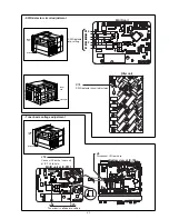
3-6-1 MATCHING CIRCUIT (TUNER UNIT)
The power supply circuit mainly consists of a 380 V DC rec-
tifier, 45 V DC switching regulator, 12, 18 V DC regulators.
When turning ON the power, the 45 V switching regulator
operates with the start-up circuit output voltage. After sever-
al milliseconds, the switching regulator operates on its own
output voltage.
3-6-2 RECTIFIER CIRCUIT
(REG, FIL-AC AND REGRELAY UNITS)
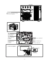
An AC voltage from the AC power socket passes through the
[POWER] swtich and is applied to the FIL-AC unit. The AC
voltage passes through the common mode filter (FIL-AC
unit; L1, L2, C2, C4–C8), and then applied to the REGRE-
LAY unit. The signal passes through R2 and R4 on the
REGRELAY unit to prevent an entry of current until 13.6 V
DC are supplied from the REG unit. After 13.6 V DC are reg-
ulated, the AC voltage bypasses R2 and R4 through RL3
and RL4 on the REGRELAY unit.
AC voltage passes through the AC filter circuit (SUBREG
unit; L4, C30, C31). The filtered signal is rectified and
smoothed by D8 and C26 on the SUBREG unit, then applied
to the AC 100/200 V select circuit (SUBREG unit; Q4, Q5,
D4) to select either 100 or 200 V AC input. The selected sig-
nal is applied to the active filter control circuit (ACTFIL unit;
IC1, pin 11) via Q7 as “SELV” signal to control output volt-
age.
AC voltage from REGRELAY unit is rectified at D1 (ACTFIL
unit), and then passes through the low-pass filter (ACTFIL
unit; L3, C35, C36). The filtered signal is applied to the
active filter circuit (REG unit; Q1–Q3, D2, L1, L2) to obtain
380 V DC output (When 100 V AC inputs, output voltage is
300 V DC), and then applied to the CONV unit via the
smoothing circuit (ACT-C unit; C1, C3, C4).
3-6-3 CONVERT CONTROL CIRCUIT
(CONV-CTRL UNIT)
Passing through a smoothing circuit, 380 V (or 300 V) DC
are applied to the invertor circuit (Q1–Q4) and are convert-
ed to a pulse signal, which is then applied to the transformer
(REG unit; T1). The signal passes through the current detec-
tor (R17, R18) to protect short-circuit.
Part of the output voltage passes through the common
mode filter (FIL-DC unit; L1, L2, C2, C4–C8), and is then
output as DC output voltage via the “HV” signal.
Part of the output voltage is rectified by D1, D2, and
smoothed by L3 (REG unit), C5, C6. The signal is amplified
at the amplifier (IC2A, pin 3), and is then applied to the limit-
ter amplifier (IC2B, pin 5). The amplified signal is compared
to “SEL” signal from the IC4, pin 4 on the SUBREG unit.
When above the thresh of IC2B, the signal from the limitter
amplifier (IC2B, pin 7) is applied to the Q14. The amplified
signal is applied to the inverter control circuit (IC1, pin 4) to
control the pulse width.
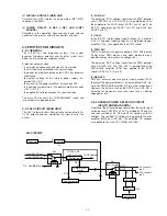
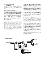
IC1 contains a reference regulator, osillator, dead-time com-
parator, PWM comparator, etc. The switching control signal
is applied to the buffer amplfier (CONV unit; Q5 or Q6).
When the switching control signal is applied to the gate ter-
minal of Q5 as “E1” signal, the amplified signal applied to the
invertor circuit (CONV unit; Q1, Q4) via the T3 on CONV
unit.
When the switching control signal is applied to the gate ter-
minal of Q6 as “E2” signal, the amplified signal applied to the
invertor circuit (CONV unit; Q2, Q3) via the T4 on CONV
unit.
380 V DC from the ACTFIL unit is switched by the invertor
circuit (CONV unit; Q1–Q4), and then applied to the T1 on
the REG unit.
16 15 14 12 7
13
10
1 2 3
4 5 6
11
8 9
Osc.
Ref.
Reg.
Low volt.
stop
T
F
F
"380H" signal from
ACT-C unit
IC2B
"SEL" signal from
IC4, pin 4 (SUBREG unit)
IC1
(Invertor control circuit)
Invertor circuit
(CONV unit; Q1—Q4)
"HVSA" signal from
IC6, pin 2 (SUBREG unit)
"12V" signal from
SUBREG unit
Q5
T3
T4
Q6
"SEL" signal from
IC4, pin 4 (SUBREG unit)
• INVERTOR CONTROL CIRCUIT
Содержание IC-PW1
Страница 1: ...SERVICE MANUAL ADDENDUM CONTENTS PARTS LIST 1 BOARD LAYOUTS 16 VOLTAGE DIAGRAM 18 Mar 2011 ...
Страница 24: ...SERVICE MANUAL ADDENDUM CONTENTS PARTS LIST 1 BOARD LAYOUTS 16 Jun 2010 ...
Страница 42: ...SERVICE MANUAL ADDENDUM CONTENTS PARTS LIST 1 BOARD LAYOUTS 16 VOLTAGE DIAGRAM 18 Apr 2010 ...
Страница 96: ...HF 50 MHz ALL BAND LINEAR AMPLIFIER iC PW1 ...
Страница 175: ...MNF F1 EP2 TO REGRELAY BOARD MLF EP1 F2 TO REGRELAY BOARD EP35 I N FG 8 19 FIL AC BOARD 8 20 ...
Страница 178: ...380G TO ACTFIL BOARD 380G 380H 380G TO CONV BOARD EP4 EP33 EP33 380H 380H EP3 EP32 EP32 EP31 8 23 8 22 ACT C BOARD ...
Страница 201: ...A 5449MZ S 3 1999 Icom Inc 1 1 32 Kamiminami Hirano ku Osaka 547 0003 Japan Count on us ...

