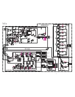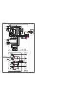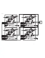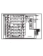
3 - 4
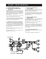
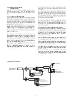
3-3-4 TEMPERATURE DETECTOR CIRCUIT
(SPLITR AND MAIN UNITS)
The temperature detector circuit detects the temperature of
the heatsink for final FETs and controls amplifying operation.
A thermistor (SPLITR unit; R16) detects temperature of the
heatsink for final FETs, and the detected temperature signal
(DC voltage) is applied to the main CPU (MAIN unit; IC26,
pin 12), to control the cooling fans and amplifying operation.
Common 5 V is applied to the thermistor for reference.
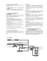
3-3-5 DRIVING FREQUENCY DETECTOR CIRCUIT
(SPLITR AND MAIN UNITS)
A portion of the RF signal from RL1 (SPLITR unit) is divided
at C18 and C19, then applied to the driving frequency detec-
tor circuit in the MAIN unit as the “F” signal.
The “F” signal from the SPLITR unit is amplified at the lim-
iter amplifier (MAIN unit; IC30) after being amplified at Q34
and Q35. The amplified signal is divided at the divider (MAIN
unit; IC20) for conversion to pulse-type signals. The signals
are applied to the main CPU (MAIN unit; IC26, pin 76). The
CPU counts the number of pulses as the driving frequency,
then controls the protector for frequency band selection.
The driving frequency detector circuit detects the input
power level at the same time to prevent malfunction at low
power level inputs.
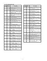
LINE
H12
12 V
5 V
+5 V
–5 V
–13 V
T13
T8V
HV
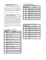
DESCRIPTION
+12 V line from the regulator circuit. The output
voltage is applied to the meter lamp (FRONT
unit; DS1, DS2).
12 V controlled from a H12 line by the relay con-
trol circuit (IC8, IC9).
5 V DC converted from a 12 V line at IC5 on the
MAIN unit. The voltage is used for the phase
detector on the DET unit.
5 V DC converted from a S12 line (+12 V) at IC6
on the FRONT unit. The voltage is used for the
output expander IC on the FRONT unit.
–5 V DC converted from a –13 V line at IC5 on
the DET board.
–13 V DC converted from a H12 (+12 V) line at
IC8 on the MAIN unit.
Transmit 13 V DC converted from a H12 (+12 V)
line at Q3 on the MAIN unit.
Transmit 8 V DC converted from a T13 line at
IC1 on the SPLITR unit. The output voltage is
used for PA1, PA2, PA3 and PA4 on the PA unit.
45 V line from the regulator circuit. The voltage is
used for PA1, PA2, PA3 and PA4 on the PA unit.
3-4 POWER SUPPLY CIRCUITS
• VOLTAGE LINE
Pin
Port
Description
number name
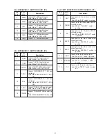
3-5 PORT ALLOCATIONS
3-5-1 EXPANDER IC (SWITCH BOARD; IC1)
4
5
11
12
13
14
I1L
I2L
A4L
A3L
A2L
A1L
Outputs INPUT “1” LED control signal.
High: While INPUT “1” LED is ON.
Outputs INPUT “2” LED control signal.
High: While INPUT “2” LED is ON.
Outputs ANT “4” LED control signal.
High: While ANT “4” LED is ON.
Outputs ANT “3” LED control signal.
High: While ANT “3” LED is ON.
Outputs ANT “2” LED control signal.
High: While ANT “2” LED is ON.
Outputs ANT “1” LED control signal
High: While ANT “1” LED is ON.
Pin
Port
Description
number name
3-5-2 EXPANDER IC (SWITCH BOARD; IC2)
4
5
6
12
13
14
VML
SML
AML
TML
IML
PML
Outputs “V
D
” LED control signal.
High: While “V
D
” LED is ON.
Outputs “SWR” LED control signal.
High: While “SWR” LED is ON.
Outputs “ALC” LED control signal.
High: While “ALC” LED is ON.
Outputs “TEMP” LED control signal.
High: While “TEMP” LED is ON.
Outputs “I
D
” LED control signal.
High: While “I
D
” LED is ON.
Outputs “P
O
” LED control signal.
High: While “P
O
” LED is ON.
Содержание IC-PW1
Страница 1: ...SERVICE MANUAL ADDENDUM CONTENTS PARTS LIST 1 BOARD LAYOUTS 16 VOLTAGE DIAGRAM 18 Mar 2011 ...
Страница 24: ...SERVICE MANUAL ADDENDUM CONTENTS PARTS LIST 1 BOARD LAYOUTS 16 Jun 2010 ...
Страница 42: ...SERVICE MANUAL ADDENDUM CONTENTS PARTS LIST 1 BOARD LAYOUTS 16 VOLTAGE DIAGRAM 18 Apr 2010 ...
Страница 96: ...HF 50 MHz ALL BAND LINEAR AMPLIFIER iC PW1 ...
Страница 175: ...MNF F1 EP2 TO REGRELAY BOARD MLF EP1 F2 TO REGRELAY BOARD EP35 I N FG 8 19 FIL AC BOARD 8 20 ...
Страница 178: ...380G TO ACTFIL BOARD 380G 380H 380G TO CONV BOARD EP4 EP33 EP33 380H 380H EP3 EP32 EP32 EP31 8 23 8 22 ACT C BOARD ...
Страница 201: ...A 5449MZ S 3 1999 Icom Inc 1 1 32 Kamiminami Hirano ku Osaka 547 0003 Japan Count on us ...

