3 - 6
The converted analog IF signal passes through the low-pass
filter (IC601, pins 3, 6, IC651, pins 3, 6), and is then applied
to the IF amplifier (IC701, pins 2, 3) to convert to unbalanc-
ing IF signal.
The 36 kHz IF signal from the IF amplifier (pin 6) is applied
to the 3rd mixer circuit.
3-2-3 3RD MIXER CIRCUIT (MAIN UNIT)
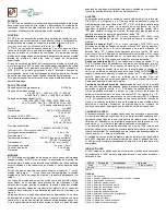
The modulated 36 kHz IF signal from the DSP-TX board
pass through the two low-pass filters (IC501, pins 3, 6,
IC502, pins 3, 6), and is then applied to the 3rd mixer circuit
(IC503, pin 3). The 36 kHz IF signal is mixed with 491 kHz
3rd LO signal (from RXPLL-A unit) to produce the 455 kHz
3rd IF signal.
The signal is amplified at the IF amplifier (Q501), and pass-
es through the one of the ceramic bandpass filters (FI501;
20 kHz, FI502; 4 kHz). The filtered signal is amplified at the
other IF amplifier (Q504), and is then applied to the 2nd
mixer circuit via the attenuator (R545–R547).
3-2-4 2ND MIXER CIRCUIT (MAIN UNIT)
The 3rd IF signal from the 3rd mixer circuit is applied to the
2nd mixer circuit (D505). The applied 3rd IF signal is mixed
with 64 MHz 2nd LO signal (from the RXPLL-A unit) to pro-
duce the 64.455 MHz 2nd IF signal.
The signal passes through the bandpass filter (FI503;
Fc=64.455 MHz) to suppress unwanted signals, and is then
applied to the IF amplifier (Q506). The 2nd IF signal is
applied to the 1st mixer circuit.
3-2-5 1ST MIXER AND RF CIRCUITS (MAIN UNIT)
The 2nd IF signal from the 2nd mixer circuit is applied to the
1st mixer circuit (D506). The 1st IF signal is mixed with 1st
LO signal (from the RXPLL-A unit) to produce the RF signal.
The RF signal passes through the low-pass filter (L518,
L519, C564–C568) and 3 dB attenuator (R578–R580). The
signal is then applied to the RF amplifier and bandpass filter
circuits.
3-2-6 RF AMPLIFIER AND BANDPASS FILTER
CIRCUITS (MAIN UNIT)
The RF signal is amplified at the RF amplifier (Q508), and
applied to the one of the 10 bandpass filters via the 5 dB
attenuator (R575–R577).
The filtered signal is applied to the YGR amplifier (Q801),
and passes through the 3 dB attenuator (R805–R807). The
signal is applied to the power amplifier circuit via the J801.
3-2-7 POWER AMPLIFIER CIRCUIT (PA200W BOARD)
The signal from the attenuator (MAIN unit; R805–R807)
passes through the 3 dB attenuator (R101–R103) via the J1,
and is then amplified at the RF amplifier (Q101). The signal
is applied to the pre-drive (Q201) and drive amplifier (Q301),
and is then amplified at the power amplifier (Q401, Q402) to
obtain 200 W output power.
The output signal is applied to the FILTER circuit via the
J401.
3-2-8 FILTER CIRCUIT (FILTER UNIT)
The power amplified signal passes through the one of the 9
low-pass filters which is depended on the RF frequencies to
suppress the unwanted frequency components. The filtered
signal is applied to the CONTROL circuit via the J904.
3-2-9 CONTROL CIRCUIT (CTRL BOARD)
The filtered signal from the FILTER unit is applied to the
SWR-DET circuit (D101, D102) to detect SWR level, and
then passes through the P-DET (D151, D152) and R-DET
circuit (D201, D202). The signal is applied to the T/R switch
(RL251), and is then applied to (or bypass) the antenna
tuner circuit (NETWORK board) via the antenna tuner selec-
tor switch (RL252, RL253).
The tuned signal from J252 (or bypass signal) passes
through the CRNT DET circuit (D301, D302) to detect the
driving current, and is then applied to the antenna switching
circuit.
The detected signal at CRNT DET circuit is amplified at the
amplifier (IC301, pin 3), and is then applied to the
TUNER_CPU (IC1, pin 16).
3-2-10 ANTENNA SWITCHING CIRCUIT
(ANT-SW UNIT)
The signal from the CTRL board is applied to the ANT-SW
unit via the J1, and is applied to the one of the 4 relays
(RL51, RL61, RL71, RL81). The signal is output from the
one of the 4 antenna connectors, J51, J61, J71 or J81.
1st LO
D506
Ceramic
filter
FI501
20 kHz
BPF
FI503
20 kHz
4 kHz
Ceramic
filter
FI502
MIC
455 kHz
DSP-TX
board
3rd LO
(491 kHz)
IF
IC503
Q501
IF
Q504
IF
Q506
BPFs
RF
Q508
to PA200W board
64.455 kHz
2nd LO
(64.00 MHz)
D505
36 kHz IF
• TRANSMITTER CONSTRUCTION
Содержание IC-7800
Страница 1: ...SERVICE MANUAL ADDENDUM CONTENTS PARTS LIST 1 BOARD LAYOUTS 65 VOLTAGE DIAGRAM 67 Dec 2009 ...
Страница 79: ...SERVICE MANUAL ADDENDUM CONTENTS PARTS LIST 1 BOARD LAYOUTS 60 VOLTAGE DIAGRAM 64 Feb 2009 ...
Страница 157: ...SERVICE MANUAL ADDENDUM CONTENTS PARTS LIST 1 BOARD LAYOUTS 57 VOLTAGE DIAGRAM 59 Aug 2008 ...
Страница 245: ...SERVICE MANUAL ADDENDUM CONTENTS PARTS LIST 1 BOARD LAYOUTS 57 VOLTAGE DIAGRAM 59 Jul 2008 ...
Страница 333: ...THE TRANSCEIVER i7800 SERVICE MANUAL S 14015HZ C1 2 Mar 2006 ...
Страница 489: ...5 10 15 20 25 30 35 40 45 50 55 60 65 0 Horizontal 5 10 15 0 25 30 35 20 40 Vertical BOTTOM VIEW MEMORY BOARD 8 12 ...
Страница 555: ...1 1 32 Kamiminami Hirano ku Osaka 547 0003 Japan S 14015HZ C1 2 C 2004 2006 Icom Inc ...


