Chapter 2. Architecture and technical overview
29
sees a single shared memory resource. They are interfaced to eight memory slots, controlled
by two SMI-II chips, which are located in close physical proximity to the processor modules.
I/O connects to the p5-520 processor module using the GX+ bus. The processor module
provides a single GX+ bus. The GX+ bus provides an interface to I/O devices through the
RIO-2 connections.
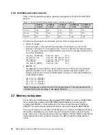
The theoretical maximum throughput of the L3 cache is 16 byte read, 16 byte write at a bus
frequency of 1.05 GHz (based on a 2.1 GHz processor clock), which equates to 33600 MBps
or 33.60 GBps. Additional throughput details are provided in Table 2-3 on page 33.
2.2.3 The p5-520Q quad-core module
The 4-core p5-520Q system planar contains a new quad-core module (QCM) and the local
memory storage subsystem for that QCM. Two dual-core processors and their
associated L3 cache are packaged in the QCM.
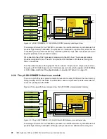
Figure 2-6 shows a layout view of a p5-520Q QCM with associated memory.
Figure 2-6 The p5-520Q 1.65 GHz QCM with DDR2 memory socket layout view
The storage structure for the processor is a distributed memory architecture that
provides high-memory bandwidth. Each processor in the QCM can address all memory and
see a single shared memory resource. In the QCM, one processor has direct
access to eight memory slots, controlled by two SMI-II chips, which are located in close
physical proximity to the processor modules. The other processor has access to
the same memory slots through the Vertical Fabric Bus.
I/O connects to the p5-520Q QCM using the GX+ bus. The QCM provides a single GX+ bus.
One processor has direct access to the GX+ Bus using its GX+ Bus controller and
the other uses the Vertical Fabric Bus controlled by the Fabric Bus controller. The GX+ bus
provides an interface to I/O devices through the RIO-2 connections.
The processor, without direct access to memory, does have a direct access to the
GX+ Bus.
The theoretical maximum throughput of the L3 cache is 16 byte read, 16 byte write at a bus
frequency of 825 MHz (based on a 1.65 GHz processor clock), which equates to 26400 MBps
or 26.4 GBps per L3 cache. There are two L3 caches on the QCM, which provide a total L3
cache bandwidth of 52800 MBps or 52.8 GBps per QCM. Additional throughput details are
provided in Table 2-3 on page 33.
SMI-II
SMI-II
1056 MHz
2 x 8B for read
2 x 2B for write
DIMM
DIMM
DIMM
DIMM
DIMM
DIMM
DIMM
DIMM
2x 8B
@528 MHz
GX+
Bus
QCM
2 x 16B
@825 MHz
36 MB
L3 cache
2 x 16B
@825 MHz
36 MB
L3 cache
Core
1.65 GHz
Core
1.65 GHz
1.9 MB
L2 cache
L3
ctrl
Mem
ctrl
Core
1.65 GHz
Core
1.65 GHz
Mem
ctrl
Enhanced
distributed switch
Enhanced
distributed switch
1.9 MB
L2 cache
L3
ctrl
GX+
Ctrl
GX+
Ctrl
SMI-II
SMI-II
1056 MHz
2 x 8B for read
2 x 2B for write
DIMM
DIMM
DIMM
DIMM
DIMM
DIMM
DIMM
DIMM
2x 8B
@528 MHz
GX+
Bus
QCM
2 x 16B
@825 MHz
36 MB
L3 cache
2 x 16B
@825 MHz
36 MB
L3 cache
Core
1.65 GHz
Core
1.65 GHz
1.9 MB
L2 cache
L3
ctrl
Mem
ctrl
Core
1.65 GHz
Core
1.65 GHz
Core
1.65 GHz
Core
1.65 GHz
Mem
ctrl
Enhanced
distributed switch
Enhanced
distributed switch
1.9 MB
L2 cache
L3
ctrl
GX+
Ctrl
GX+
Ctrl
GX+
Ctrl
GX+
Ctrl
Содержание REDPAPER 520Q
Страница 2: ......
Страница 8: ...vi IBM System p5 520 and 520Q Technical Overview and Introduction...
Страница 14: ...xii IBM System p5 520 and 520Q Technical Overview and Introduction...
Страница 38: ...24 IBM System p5 520 and 520Q Technical Overview and Introduction...
Страница 104: ...90 IBM System p5 520 and 520Q Technical Overview and Introduction...
Страница 108: ...94 IBM System p5 520 and 520Q Technical Overview and Introduction...
Страница 109: ......


