110
IBM Power System E850C: Technical Overview and Introduction
4.3.10 Memory protection
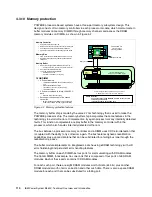
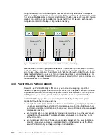
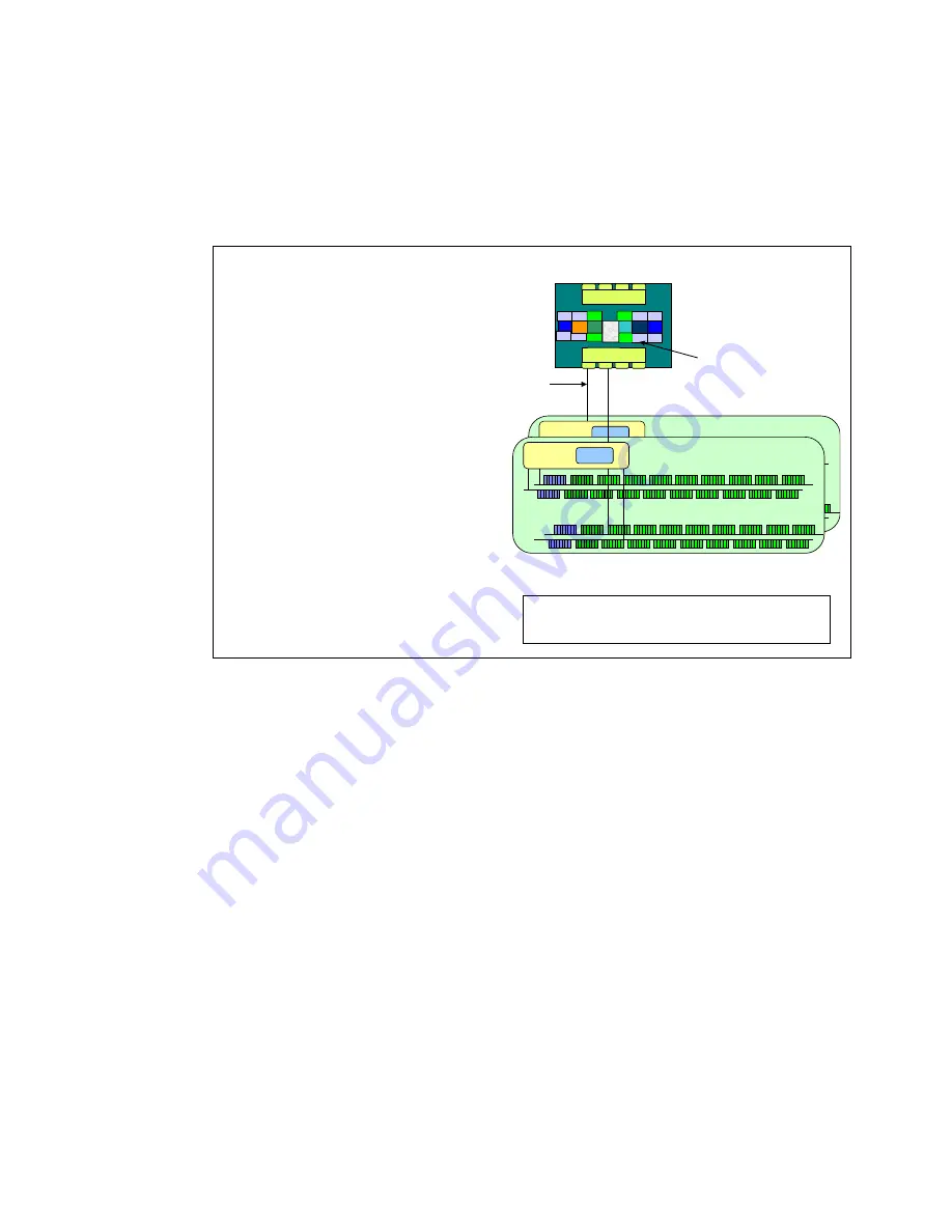
POWER8 processor-based systems have a three-part memory subsystem design. This
design consists of two memory controllers in each processor module, which communicate to
buffer modules on memory DIMMS through memory channels and access the DRAM
memory modules on DIMMs, as shown in Figure 4-2.
Figure 4-2 Memory protection features
The memory buffer chip is made by the same 22 nm technology that is used to make the
POWER8 processor chip. The memory buffer chip incorporates the same features in the
technology to avoid soft errors. It implements a try again process for many internally detected
faults. This function complements a replay buffer in the memory controller within the
processor, which also handles internally detected soft errors.
The bus between a processor memory controller and a DIMM uses CRC error detection that
is coupled with the ability to try soft errors again. The bus features dynamic recalibration
capabilities plus a spare data lane that can be substituted for a failing bus lane through the
recalibration process.
The buffer module implements an integrated L4 cache using eDRAM technology (with soft
error hardening) and persistent error handling features.
The memory buffer on each DIMM has four ports for communicating with DRAM modules.
The 16 GB DIMM, for example, has one rank that is composed of four ports of x8 DRAM
modules. Each of these ports contains 10 DRAM modules.
For each such port, there are eight DRAM modules worth of data (64 bits) plus another
DRAM module’s worth of error correction and other such data. There is also a spare DRAM
module for each port that can be substituted for a failing port.
L4 Cache
Memory
Buffer
L4
Memory Controller
Supports 128 Byte Cache Line
Hardened “Stacked” Latches for Soft Error Protection
And reply buffer to retry after soft internal faults
Special Uncorrectable error handling for solid faults
Memory Bus
CRC protection with recalibration and retry on error
Spare Data lane can be dynamically substituted for
failed one
Memory Buffer
Same technology as POWER8 Processor Chips
–
Hardened “Stacked” Latches for Soft Error Protection
Can retry after internal soft Errors
L4 Cache implemented in eDRAM
–
DED/SEC ECC Code
–
Persistent correctable error handling
16 GB DIMM
4 Ports of Memory
–
10 DRAMs x8 DRAM modules attached to each
port
–
8 Modules Needed For Data
–
1 Needed For Error Correction Coding
–
1 Additional Spare
2 Ports are combined to form a 128 bit ECC
word
–
8 Reads fill a processor cache
Second port can be used to fill a second
cache line
–
(Much like having 2 DIMMs under one Memory
buffer but housed in the same physical DIMM)
L4 Cache
Memory
Buffer
L4
1 Rank DIMM Supporting 2
128 Bit ECC word DRAM Groups
Memory Ctrl
POWER8 DCM with
8 Memory Buses
Supporting 8 DIMMS
Note: Bits used for data and for ECC are spread across
9 DRAMs to maximize error correction capability
Memory Ctrl
Memory Bus
DRAM Protection:
Can handle at least 2 bad x8 DRAM modules across two ports
comprising an ECC word
(3 if not all 3 failures on the same port)
128 Byte Cache Line
Содержание E850C
Страница 2: ......
Страница 36: ...22 IBM Power System E850C Technical Overview and Introduction...
Страница 114: ...100 IBM Power System E850C Technical Overview and Introduction...
Страница 154: ...140 IBM Power System E850C Technical Overview and Introduction...
Страница 158: ...144 IBM Power System E850C Technical Overview and Introduction...
Страница 159: ......
Страница 160: ...ibm com redbooks Printed in U S A Back cover ISBN 0738455687 REDP 5412 00...

