


VHF (136-174 MHz)
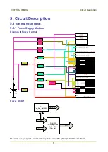
Circuit Description
20
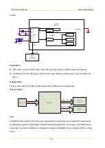
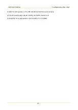
Drive-stage
Final-stage
Tx/Rx Switch
Microstrip
Matcher
TV/APC
Gate voltage control
Subtracter
Gain:14dB
Po(max):29dBm
static I
d:120mA
Gain:10dB
Po(max):38.5dBm
static I
d:200mA
S11:< -15dB(140MHZ bandwidth)
S21: < -0.5dB
S21:-0.2dB
S21:< -0.8dB
BW(-3dB):570MHZ
Stop band attenuation :-54dBc
Sampling
resistor
I/V
convertor
Gain:18dB
Po(-1dB):15.5dBm
static Ic:25mA
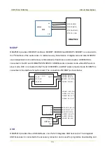
Pre-driver1
Pi Attenuator
1
2
ATT:-10dB
S21: < -
0.5dB
S21: < -
0.5dB
PI MATCH
BATT+
TX_VCO
DAC
TLV5614
ANT
RX/TX
VCO Buffer
RX/TX
VCO Amplifier
LPF
APC
MODULE
TV/APC
OMAP
MCBSP2
RF Power Amplifier Circuit
The carrier signal generated by TX VCO is first to be modulated and amplified, and then feeds to the
transmitter circuit. See the steps below.
Step 1
In this cir
cuit, the signal passes through a π
-type attenuator first, allowing certain isolation
between the RF power amplifier circuit and TX VCO.
Step 2
After that, the signal goes to the driver amplifier (RD01) for further power amplification, to
provide appropriate amplication signal to the final-stage amplifier (RD07) for final power amplification.
Step 3
After amplified by multiple amplifiers, the signal will pass through a microstrip matcher to
complete output impedance matching, so as to reduce output power loss due to impedance mismatch.
Step 4
Finally, the signal passes through the TX/RX switch and goes to the low-pass filter.
Low-pass Filter Circuit (for suppressing harmonics)
The low-pass filter for suppressing harmonics is a high-order Elliptic filter composed of
lumped-parameter inductors and capacitors. Via this filter, the spurious signal within the stop band can
be attenuated as much as possible while the in-band ripple is within the required range.
Auto Power Control Circuit
In the auto power control and temperature detection circuit, the drain current from the driver amplifier
and final-stage amplifier is converted to voltage via the sampling resistor and subtraction circuit
(composed of the first operational amplifier).
This voltage is compared with the APC control voltage (output by DAC) at the second operational
amplifier. Then the output error voltage controls TX power by controlling the compensated gate bias
voltage of the amplifiers (including the driver amplifier and the final-stage amplifier).
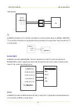
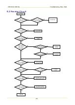
5.2.2
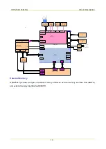
Receiver Circuit
The receiver circuit mainly comprises the RF band-pass filter, low-noise amplifier, mixer, IF filter, IF
amplifier and IF processor.
Содержание PD502
Страница 1: ...PORTABLE...
Страница 5: ...VHF 136 174 MHz...
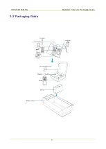
Страница 13: ...VHF 136 174 MHz Exploded View and Packaging Guide 7 3 2 Packaging Guide...
Страница 18: ...VHF 136 174 MHz Circuit Description 12...
Страница 43: ...PCB 3 9 PCB VHF 136 174 MHz...
Страница 44: ...PCB 3 VHF 136 174 MHz...
Страница 71: ...UHF1 400 470 MHz...
Страница 79: ...UHF1 400 470MHz Exploded View and Packaging Guide 7 3 2 Packaging Guide...
Страница 84: ...UHF1 400 470MHz Circuit Description 12...
Страница 108: ...UHF1 400 470MHz PCB 36 9 PCB...
Страница 109: ...UHF1 400 470MHz PCB 37...
Страница 136: ...1616300000260 2014 03 17 L07157 4...