background image

MAN1175-01-EN

Indianapolis, USA  |  Cork, Ireland  |  Calgary, Canada  |  Bangalore, India  |  Oakleigh, Australia  |  Tianjin, China  |  Esteio, Brazil

Please visit our website for a complete listing and to learn more about certified Horner Automation products.
This document is the property of Horner Automation Group, and is subject to change. 

page 5 of 8


4  CSCAPE CONFIGURATION 

The HE959CNX116 Base is configured from Cscape, under “Hard-
ware Configuration”. Cscape 9.9 (SP8 or later) is required. OCS 
firmware must be updated to support OCS-I/O.  Please check the 
release notes on your OCS model to ensure OCS-I/O support is 
included.  

General configuration procedure:

1.    In Cscape, select Controller > Hardware Configuration.
2.   Make sure the OCS controller to be used in the application   
      has been properly selected.
3.   Select the “CsCAN I/O” Tab.
4.   Click the “Add” Button
5.   Select “HE959CNX116” in the OCS-I/O tab
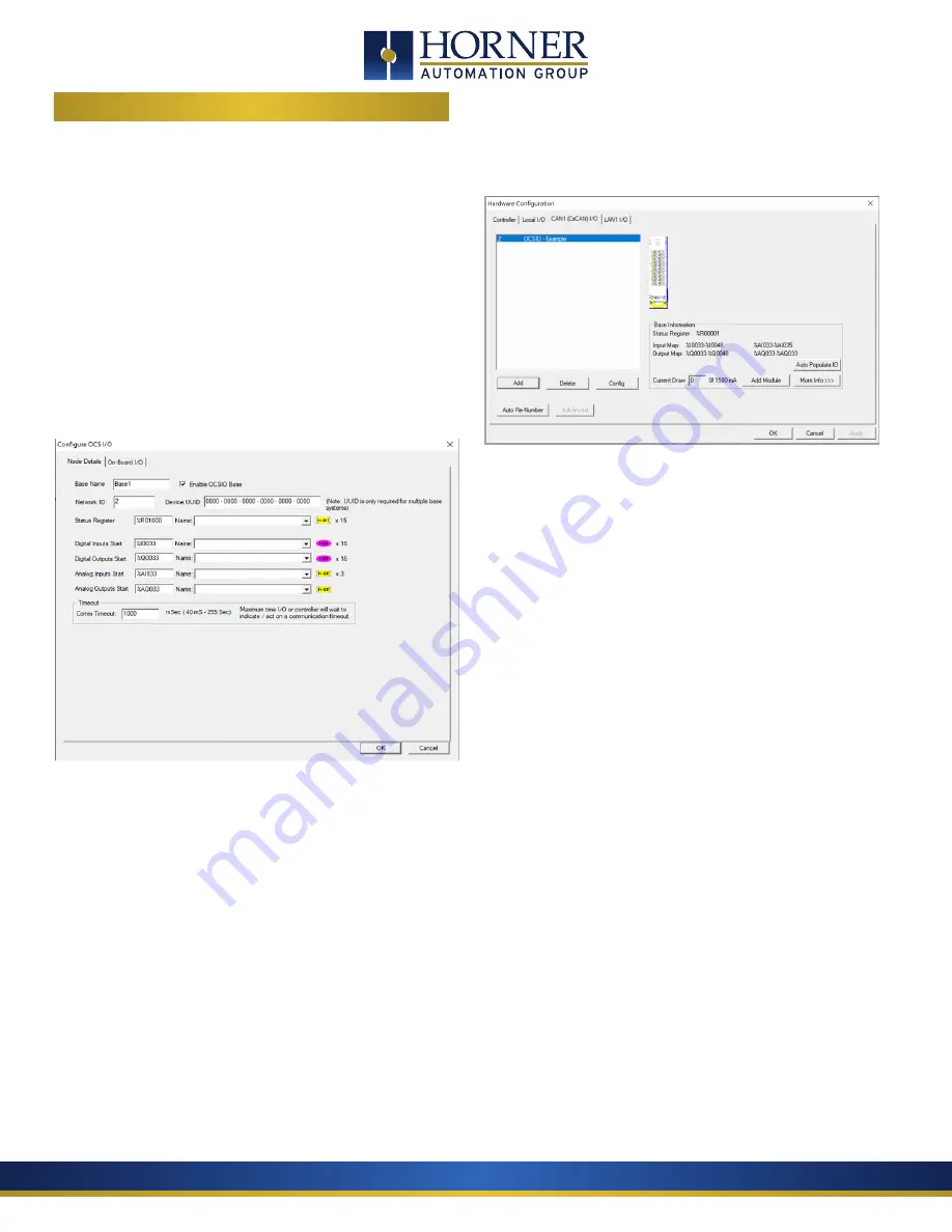
6.  Click the “OK” button. This opens the following dialog: 

• 

Base Name

 – any descriptive text (up to 15 characters)

• 

Enable OCSIO 

- When this option is checked Input/Output 

data from the host controller will get transmitted to OCSIO. 
If the option is unchecked Input /Output data will NOT get 
transmitted to OCSIO but communication between the Host 
controller and OCSIO will be healthy

• 

Network ID 

– unique CsCAN ID (

1-79

 decimal)

• 

Device UUID -

 Each OCSIO base requires a Unique ID to 

establish communication with the host controller. In case 
of Single Base OCSIO entering UUID is not required, host 
controller can automatically assign that. In case of Multiple 
base configurations, it is Mandatory to enter UUID of each 
base.

• 

Status Register 

– Location where fifteen consecutive words 

are reported

• 

Digital Inputs / Digital Outputs / Analog Inputs / Analog 
Outputs Start

 – starting locations for each type of I/O for 

this base.  Be careful to choose starting addresses that do 
not conflict with OCS built-in I/O mapping.

• 

Comm Timeout 

– Maximum amount of time the 

HE959CNX116  will wait to act on a communications timeout 
(40 to 255000ms)

7.   After entering all the required information (above), click “OK”.      
     At this point, the following Hardware Configuration dialog will    
     appear:

8.  Now modules can be added via the “Add Module” button. As        
I/O modules are added the Input Map, Output Map, and Current    
Draw are updated, showing the accumulated I/O Module Informa-
tion. More details regarding each module can be viewed via the 
“More Info” button.

9. If the OCS-I/O base and I/O modules are properly connected 
and powered up, and if Cscape currently has communications to 
the OCS, the “Auto Populate IO” button may be used to recognize 
all modules installed on this OCS-I/O base.

10.   Right clicking on an I/O module will allow detailed configura- 
tion to be performed, as follows:
 

a.     Digital Input modules can be configured to update  


on a change of state (typical) or periodically (rare). Input  


filtering can also be adjusted from the default of 1mS.


b.  Digital Output modules can optionally be configured  


to hold last state in Stop/Idle mode.


c. Analog Input modules can be configured with an    


update rate of 10mS to 255 seconds. Analog Inputs also  


have configurable data type and range which varies by  


module type.


d. Analog Output modules have configurable type and  


range, and also can have Stop/Idle behavior adjusted to  


Hold Last State, or go to Minimum (default), Medium or  


Maximum value.

11. 

Press “OK” to complete the process.

Содержание HE959CNX116

Страница 1: ...es 0 10V 0 20mA 4 20mA 0 60mV 0 10V 0 20mA 4 20mA 0 60mV 16 Bit AI Full Scale 0 20 Thermocouple J K T N E R S B Converter Type 16 Bit ADC RTD PT100 PT1000 RTD Excitation Current 250mA 1 4 Digital Outputs Inputs per Module 2 Commons per Module 1 Output Type Sourcing with 10kΩ pull down Absolute Max Voltage 28VDC Output Protection Short Circuit Max Output per Point 2A Max Total Out Current 4A Max Ou...

Страница 2: ...ld be followed in the installation of this product b Shielded twisted pair wiring should be used for best performance c Shields should be grounded at one end only preferably at the end providing the best noise shunting SAFETY PART NUMBER HE959CNX116 TECHNICAL SUPPORT For assistance and manual updates contact Technical Support at the following locations North America Europe 317 916 4274 353 21 4321...

Страница 3: ...uts Digital Analog Number of Channels 2 Digital or Analog Configured as Analog I O Analog Input Ranges 4 20mA 0 10V Analog Input Data Ranges 0 4000 2000 2000 0 1000 0 32000 Alarm Value Register Configured to Digital Inputs Digital Input Ranges 24V 12V 5V Custom Input Voltage Range 0 24VDC Absolute Max Voltage 30VDC Input Impedance 10kΩ Custom Digital Input Ranges Threshold ON Threshold OFF OFF to ...

Страница 4: ...only usually at the DC supply powering the network The network DC supply should have its V terminal connected directly to earth ground If multiple DC supplies are used to power the network the V from any one supply should be connected only to nodes it is powering disconnected from other sections powered by other supplies The V connection should be continuous across the entire network although V sh...

Страница 5: ...Q 0 10V Analog Out 10VDC 4 20 mA Analog Out OV AQ 20mA Digital Analog In 24V 12V 5V Custom Current Mode I1 0V 20mA Digital Out Positive Logic vs Negative Logic Wiring The OCS can be wired for positive or negative logic inputs 0V I1 0V I1 Positive Logic In Negative Logic In 0 10VDC Voltage Mode I1 0V Universal Analog Input 1a 1b 1c 0 10VDC NC 0 10V Analog In 1c 1a 1b 60mV 60mV mV In NC Thermocouple...

Страница 6: ...D of each base Status Register Location where fifteen consecutive words are reported Digital Inputs Digital Outputs Analog Inputs Analog Outputs Start starting locations for each type of I O for this base Be careful to choose starting addresses that do not conflict with OCS built in I O mapping Comm Timeout Maximum amount of time the HE959CNX116 will wait to act on a communications timeout 40 to 2...

Страница 7: ...guration mismatch error of each IO Modules Module 1 to Module 8 IOE Each bit bit9 bit 16 represents IO modules error Module 1 to Module 8 WDG TRIP IO base watchdog trip count IOCS Each bit bit9 bit 16 represents IO modules calibration status Module 1 to Module 8 PUP Power up error sticky bit OFFLINE OCSIO is offline DI1 US High when Digital input 1 is in undefined state DI2 US High when Digital in...

Страница 8: ... ON Flash 1Hz OCS Run Mode ON ANY ANY ANY Onboard I O Fault ON OFF ON ON Invalid Dynamic Configuration ON Flash 1Hz ON ON Power Up Waiting to be Configured ON ON Flash 1Hz Flash 1Hz LED Indicators for Individual I O Channels I1 Digital Input 1 active I2 Digital Input 2 active Q1 Digital Output 1 active Q2 Digital Output 2 active AI1 Analog Input Active AQ1 Analog output Active NOTE Channel LED wil...

Отзывы: