


Rev. 2.50
��0
��ne 22� 20��
Rev. 2.50
���
��ne 22� 20��
HT66F20/HT66F30/HT66F40/HT66F50/HT66F60
HT66FU30/HT66FU40/HT66FU50/HT66FU60
A/D Flash MCU with EEPROM
HT66F20/HT66F30/HT66F40/HT66F50/HT66F60
HT66FU30/HT66FU40/HT66FU50/HT66FU60
A/D Flash MCU with EEPROM
Register Name
Bit
7
6
5
4
3
2
1
0
ADRL(ADRFS=0)
D3
D2
D�
D0
—
—
—
—
ADRL(ADRFS=�)
D�
D6
D5
D4
D3
D2
D�
D0
ADRH(ADRFS=0)
D��
D�0
D9
D8
D�
D6
D5
D4
ADRH(ADRFS=�)
—
—
—
—
D��
D�0
D9
D8
ADCR0
START
EOCB
ADOFF
ADRFS
ACS3
ACS2
ACS�
ACS0
ADCR�
ACS4
V�25EN
—
VREFS
—
ADCK2
ADCK�
ADCK0
ACERL
ACE�
ACE6
ACE5
ACE4
ACE3
ACE2
ACE�
ACE0
ACERH
—
—
—
—
ACE��
ACE�0
ACE9
ACE8
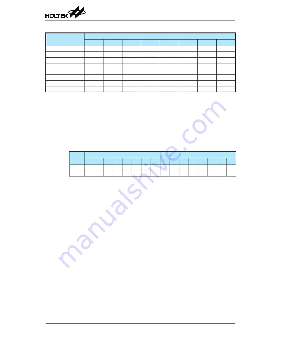
HT66F60 A/D Converter Register List
A/D Converter Data Registers – ADRL, ADRH
As the devices contain an internal 12-bit A/D converter, they require two data registers to store the
converted value. These are a high byte register, known as ADRH, and a low byte register, known
as ADRL. After the conversion process takes place, these registers can be directly read by the
microcontroller to obtain the digitised conversion value. As only 12 bits of the 16-bit register space
is utilised, the format in which the data is stored is controlled by the ADRFS bit in the ADCR0
register as shown in the accompanying table. D0~D11 are the A/D conversion result data bits. Any
unused bits will be read as zero.
ADRFS
ADRH
ADRL
7
6
5
4
3
2
1
0
7
6
5
4
3
2
1
0
0
D�� D�0 D9 D8 D� D6 D5 D4 D3 D2 D� D0
0
0
0
0
�
0
0
0
0
D�� D�0 D9 D8 D� D6 D5 D4 D3 D2 D� D0
A/D Data Registers
A/D Converter Control Registers – ADCR0, ADCR1, ACERL, ACERH
To control the function and operation of the A/D converter, three or four control registers known as
ADCR0, ADCR1, ACERL and ACERH are provided. These 8-bit registers define functions such
as the selection of which analog channel is connected to the internal A/D converter, the digitised
data format, the A/D clock source as well as controlling the start function and monitoring the A/D
converter end of conversion status. The ACS3~ACS0 bits in the ADCR0 register and ACS4 bit is
the ADCR1 register define the ADC input channel number. As the device contains only one actual
analog to digital converter hardware circuit, each of the individual 8 or 12 analog inputs must be
routed to the converter. It is the function of the ACS4~ACS0 bits to determine which analog channel
input pins or internal 1.25V is actually connected to the internal A/D converter.
The ACERH and ACERL control registers contain the ACER11~ACER0 bits which determine
which pins on Port A, PE6, PE7, PF0 and PF1 are used as analog inputs for the A/D converter input
and which pins are not to be used as the A/D converter input. Setting the corresponding bit high will
select the A/D input function, clearing the bit to zero will select either the I/O or other pin-shared
function. When the pin is selected to be an A/D input, its original function whether it is an I/O or
other pin-shared function will be removed. In addition, any internal pull-high resistors connected to
these pins will be automatically removed if the pin is selected to be an A/D input.