


Rev. 1.10
10
March 02, 2020
Rev. 1.10
11
March 02, 2020
BS83A02L/BS83B04L
Ultra-Low Power Touch Key Flash MCU
BS83A02L/BS83B04L
Ultra-Low Power Touch Key Flash MCU
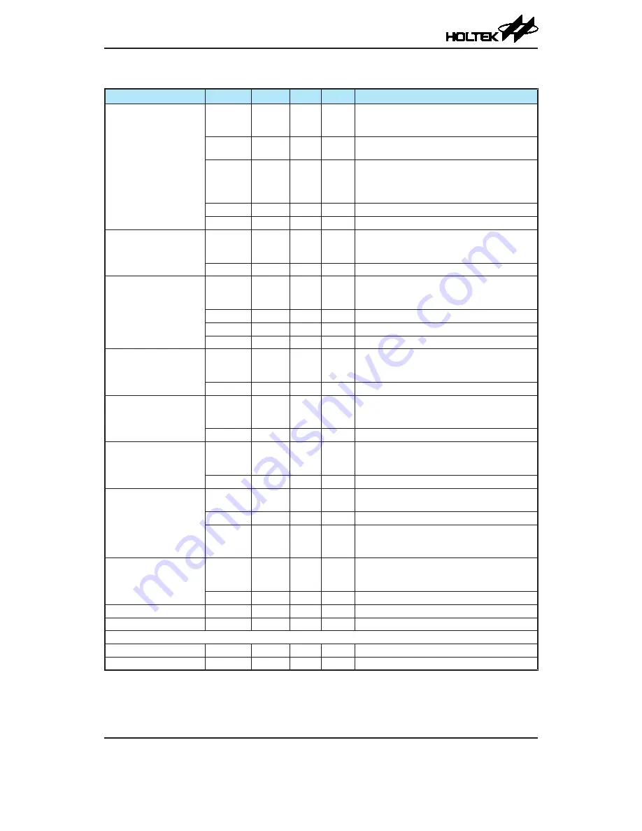
BS83B04L
Pin Name
Function
OPT
I/T
O/T
Description
PA0/CTCK/INT/SCL/
ICPDA
PA0
PAPU
PAWU
PAS0
ST
CMOS General purpose I/O. Register enabled pull-up
and wake-up
CTCK
PAS0
IFS
ST
—
CTM clock input
INT
PAS0
IFS
INTEG
INTC0
ST
—
External Interrupt input
SCL
PAS0
ST
NMOS I
2
C clock line
ICPDA
—
ST
CMOS ICP data/address
PA1/KEY2
PA1
PAPU
PAWU
PAS0
ST
CMOS General purpose I/O. Register enabled pull-up
and wake-up
KEY2
PAS0
AN
—
Touch key input
PA2/CTPB/SDA/ICPCK
PA2
PAPU
PAWU
PAS0
ST
CMOS General purpose I/O. Register enabled pull-up
and wake-up
CTPB
PAS0
—
CMOS CTM inverted output
SDA
PAS0
ST
NMOS I
2
C data line
ICPCK
—
ST
—
ICP clock pin
PA3/KEY3
PA3
PAPU
PAWU
PAS0
ST
CMOS General purpose I/O. Register enabled pull-up
and wake-up
KEY3
PAS0
AN
—
Touch key input
PA4/KEY4
PA4
PAPU
PAWU
PAS1
ST
CMOS General purpose I/O. Register enabled pull-up
and wake-up
KEY4
PAS1
AN
—
Touch key input
PA5/KEY1
PA5
PAPU
PAWU
PAS1
ST
CMOS General purpose I/O. Register enabled pull-up
and wake-up
KEY1
PAS1
AN
—
Touch key input
PA6/CTCK/INT
PA6
PAPU
PAWU
ST
CMOS General purpose I/O. Register enabled pull-up
and wake-up
CTCK
IFS
ST
—
CTM clock input
INT
IFS
INTEG
INTC0
ST
—
External Interrupt input
PA7/CTP
PA7
PAPU
PAWU
PAS1
ST
CMOS General purpose I/O. Register enabled pull-up
and wake-up
CTP
PAS1
—
CMOS CTM output
VDD
VDD
—
PWR
—
Power supply
VSS
VSS
—
PWR
—
Ground
For 16-pin NSOP package type only
OCDSDA
OCDSDA
—
ST
CMOS OCDS data/address pin, for EV chip only
OCDSCK
OCDSCK
—
ST
—
OCDS clock pin, for EV chip only
Legend: I/T: Input type;
O/T: Output type;
OPT: Optional by register selection;
PWR: Power;
ST: Schmitt Trigger input;
CMOS: CMOS output;
NMOS: NMOS output;
AN: Analog signal.