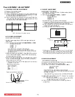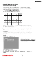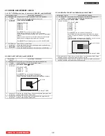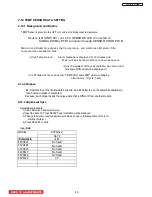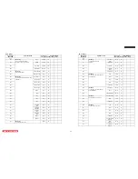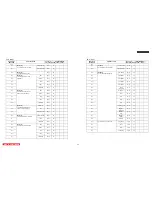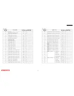
2-8 GAMMA Correction (White Balance)
GAMMA data (white balance) should not be adjusted. This data are adjusted by the factory
and MEMORY INITialize cannot erase these data. If and only if the customer request to
change the GAMMA correction, follow the instruction below.
(1) Heat run for 10 minutes or more after power on.
(2) The white signal is generated from the internal IC.
(3) Change only the step that are requested to change.
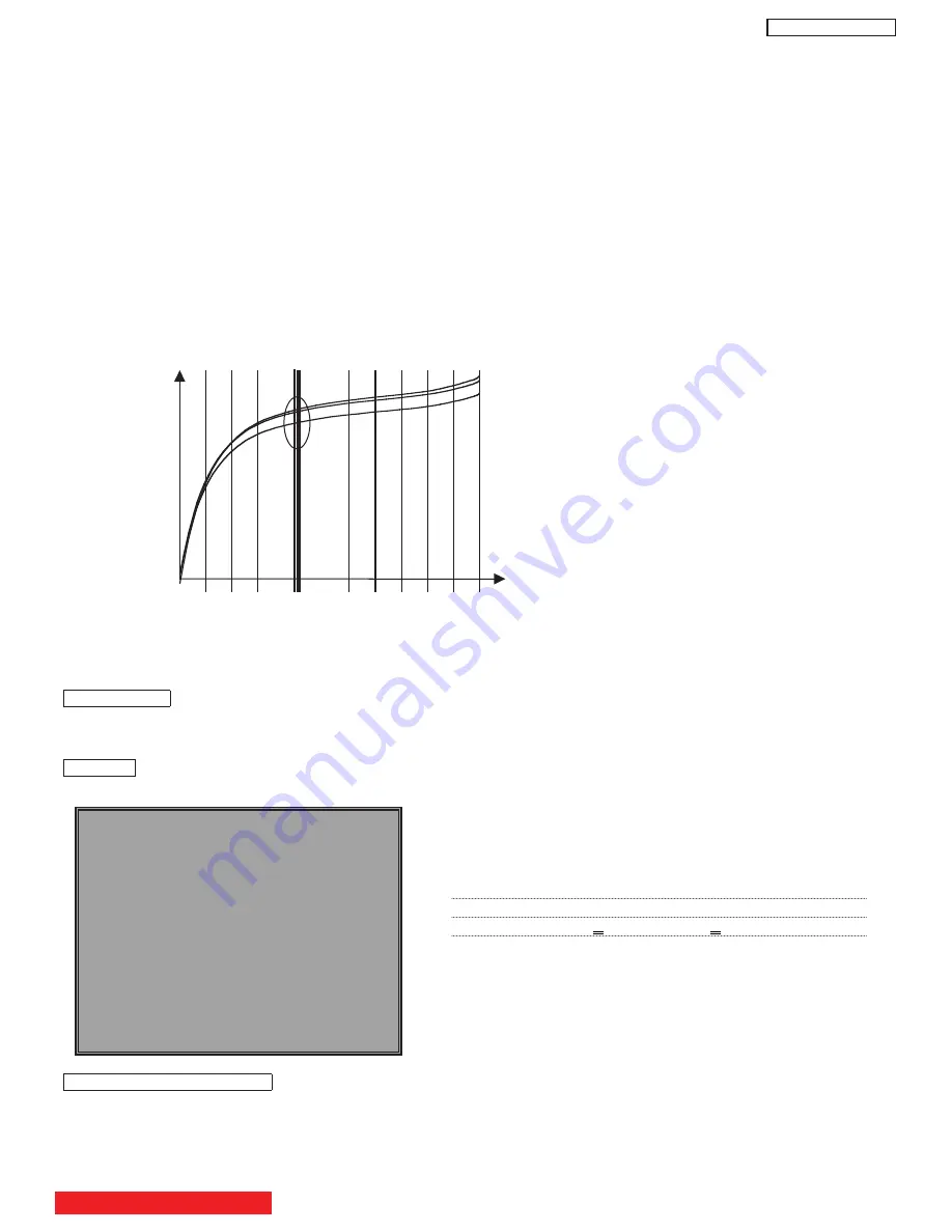
For customer request, it is possible to adjust RGB signal amplitude (means adjust the
gamma correction curve) each signal level (No.1
_
No.32).
If customer require to change the white balance of LCD PTV, we should re-adjust gamma
correction curve.
No.0
_
1 2 3 12 27 28 29 30 31 32
1. ADJUSTMENT PROCEDURE for SERVICE
Input signal level(luminance level) is divided into 32(No.0
_
No.32).
FOR EXAMPLE,
If customer require to change the white balance of 12
th
level of white to reddish, increase
the red value and adjust the white balance of 12
th
signal level (see below).
I 2C MENU
LCDADJ>GAMMA>No.12
(Adjustment)
S TORE THE DATA TO TV SET
LCD ADJ>G/C WRITE
_
press for several second
After this procedure, this new data will be write back to E2PROM. It takes about 20
seconds (picture will be black out).
INPUT SIGNAL LEVEL (A/32step)
For GAMMA CORRECTION
RED GAMMA CORRECTION CURVE
GREEN GAMMA CORRECTION CURVE
BLUE GAMMA CORRECTION CURVE
LCD ADJUST
GAM No.12
R
126->increase this data
G
138
B
105
Final ASSEMBLY ADJUSTMENT
Remark: The gamma data for higher intensity should
always be bigger than that of lower intensity. If
not, noise may appear on the screen.
example:
GAM No11
GAM No12
GAM No13
R
120
>
119
<
127
NG
R
120
<
128
>
127
NG
R
120
<
125
<
127
OK
GAM No12 Red Adjustable Range 120~127
LC58/LC58E
BACK TO ADJUSTMENTS
36
Содержание 50VF820 - 50" Rear Projection TV
Страница 96: ...LC58 LC58E CIRCUIT BLOCK DIAGRAM TABLE OF CONTENTS 96 ...
Страница 97: ...LC58 LC58E POWER SUPPLY BLOCK DIAGRAM TABLE OF CONTENTS 97 ...
Страница 98: ...CONNECTION DIAGRAM TABLE OF CONTENTS LC58 LC58E 98 ...
Страница 105: ...LC58 chassis Model 50VF820 55VF820 60VF820 1 FRONT PANEL 2 REAR PANEL LC58 LC58E 105 ...
Страница 106: ...LC58E chassis Model 50VG825 55VG825 60VG825 1 FRONT PANEL 2 REAR PANEL LC58 LC58E 106 ...
Страница 110: ...TABLE OF CONTENTS FINAL WIRING DIAGRAM TABLE OF CONTENTS TABLE OF CONTENTS LC58 LC58E 110 Model 55VF820 Model 55VG825 ...
Страница 125: ...LC58 LC58E WAVEFORMS AT EACH SECTION PST Pin 63 SDA PST Pin 64 SCL 25 26 Click on number to go to schematic 125 ...
Страница 155: ...SIGNAL PWB Solder side PRINTED CIRCUIT BOARDS BACK TO TABLE OF CONTENTS LC58 LC58E 155 ...
Страница 159: ...PRINTED CIRCUIT BOARDS POWER PWB Solder side BACK TO TABLE OF CONTENTS LC58 LC58E 159 ...
Страница 162: ...PRINTED CIRCUIT BOARDS DOOR SW A PWB Component side Solder side BACK TO TABLE OF CONTENTS LC58 LC58E 162 ...
Страница 163: ...PRINTED CIRCUIT BOARDS DOOR SW B PWB Component side Solder side BACK TO TABLE OF CONTENTS LC58 LC58E 163 ...
Страница 167: ...PRINTED CIRCUIT BOARDS PJIG A PWB Solder side BACK TO TABLE OF CONTENTS LC58 LC58E Component side 167 ...
Страница 168: ...PRINTED CIRCUIT BOARDS PJIG C PWB BACK TO TABLE OF CONTENTS LC58 LC58E Solder side Component side IJC1 IC 168 ...
Страница 169: ...PRINTED CIRCUIT BOARDS TACT SW PWB BACK TO TABLE OF CONTENTS LC58 LC58E Component side Solder side 169 ...
Страница 190: ......

