background image

VMIVME-2533 Differential Digital Output Board

10

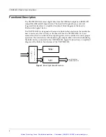
Functional Block Diagram

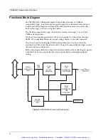
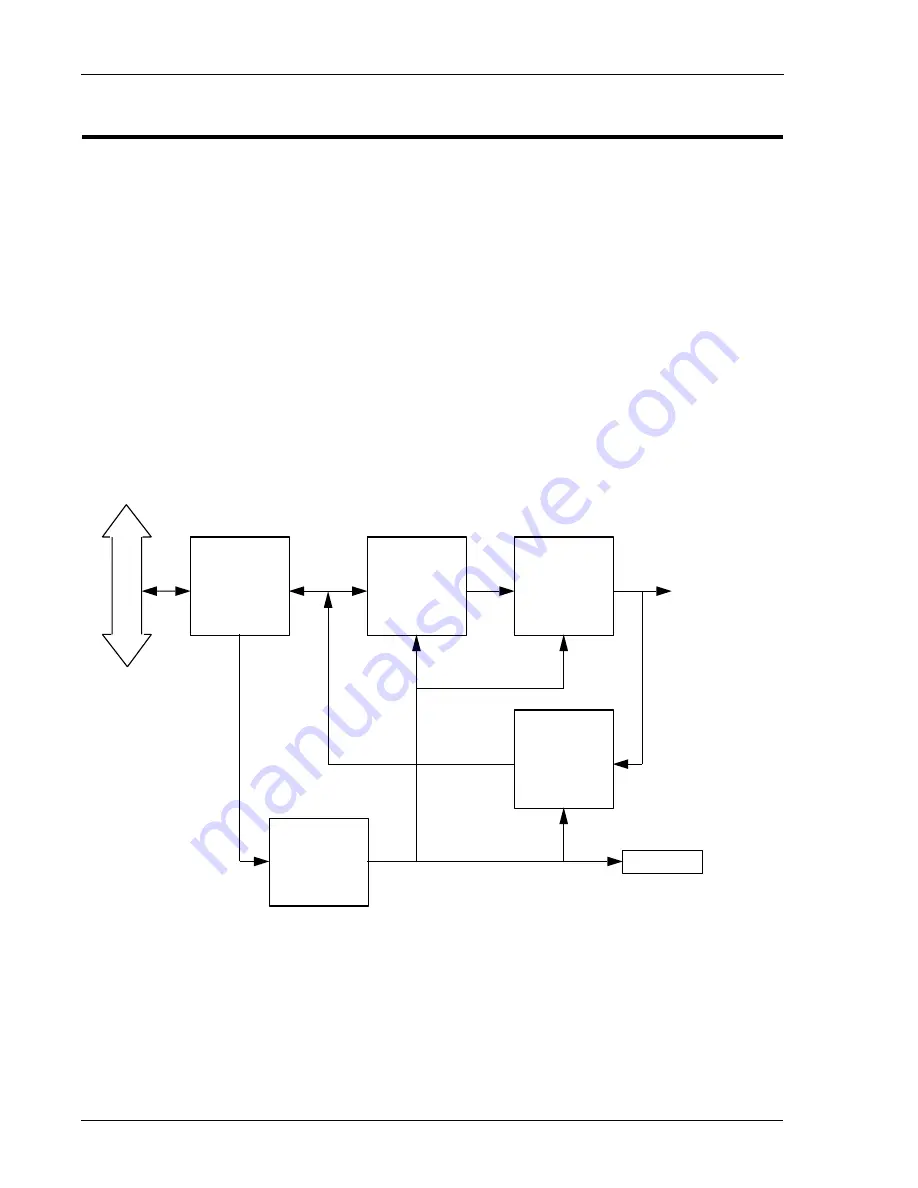
The VMIVME-2533 Differential Digital Output Board consists of VMEbus 
compatibility logic, four 8-bit output registers, eight 4-bit differential line drivers, a 
Control and Status Register, and eight 4-bit differential line receivers used by the 
Built-in-Test logic, as shown in Figure 3 below.

The VMEbus compatibility logic controls data transfer allowing 8-, 16-, or 32-bit 
VMEbus data transfers.

The four 8-bit output registers latch 32 bits of output data, which drives the eight 
RS485/422 compatible differential output voltage drivers to the field connector.

The Control and Status Register (CSR) contains three bits. One bit controls the 
on-board Fail LED, while the other two bits, along with some additional logic, control 
the test functions of the board.

Built-in-Test logic enables the output data to be read back without affecting the signals 
to the field. System reset puts the board into test mode for immediate loopback 
testing.

Figure 3  

VMIVME-2533 Functional Block Diagram

VMEbus 

FOUNDATION 

LOGIC


s

FOUR 

8-BIT 

OUTPUT 

REGISTERS

DATA 

BUS

EIGHT 

4-BIT 

DIFFERENTIAL 

LINE DRIVERS

32 

DIFFERENTIAL 

OUTPUTS

EIGHT 

4-BIT 

DIFFERENTIAL 

LINE 

RECEIVERS

FAIL LED

CSR AND 

CONTROL 

LOGIC


S

Artisan Technology Group - Quality Instrumentation ... Guaranteed | (888) 88-SOURCE | www.artisantg.com

Содержание VMIVME-2533 Series

Страница 1: ...l service in house repair center WE BUY USED EQUIPMENT Sell your excess underutilized and idle used equipment We also offer credit for buy backs and trade ins www artisantg com WeBuyEquipment REMOTE INSPECTION Remotely inspect equipment before purchasing with our interactive website at www instraview com LOOKING FOR MORE INFORMATION Visit us on the web at www artisantg com for more information on ...

Страница 2: ...ligent Platforms Publication No 500 002533 000 Rev L Hardware Reference VMIVME 2533 Differential Digital Output Board Artisan Technology Group Quality Instrumentation Guaranteed 888 88 SOURCE www artisantg com ...

Страница 3: ...Document History Hardware Reference Document Number 500 002533 000 Rev L May 25 2010 Artisan Technology Group Quality Instrumentation Guaranteed 888 88 SOURCE www artisantg com ...

Страница 4: ...ust Alone 12 Do Not Substitute Parts or Modify System 12 Dangerous Procedure Warnings 12 Safety Symbols Used in This Manual 13 Chapter 1 Theory of Operation 14 Operational Overview 15 VMEbus Compatibility Logic 16 Device Addressing 17 Built In Test Description 21 Chapter 2 Configuration and Installation 22 Jumper Configuration 23 Address Modifiers 24 Data Registers Base Address 25 CSR Base Address...

Страница 5: ...ront Panel Connector Configuration 27 Chapter 3 Programming 31 Data Output 32 Data Loopback 33 Control and Status Register CSR 34 Maintenance 39 Artisan Technology Group Quality Instrumentation Guaranteed 888 88 SOURCE www artisantg com ...

Страница 6: ...ock Diagram 18 Figure 1 4 Data Transfer Block Diagram 19 Figure 1 5 CSR Block Diagram 20 Figure 2 1 Jumper Locations 23 Figure 2 2 Address Modifier Positions 24 Figure 2 3 Data Registers Base Address Configuration 25 Figure 2 4 CSR Base Address Configuration 26 Figure 2 5 Cable Connector Configuration 27 Figure 2 6 P3 Connector Pin Layout 28 Figure 2 7 P1 P2 Connector Pin Layout 30 Artisan Technol...

Страница 7: ...ist of Tables Table 2 1 P3 Output Connector Channel Assignments 29 Table 3 1 Address Register Bit Definitions 33 Artisan Technology Group Quality Instrumentation Guaranteed 888 88 SOURCE www artisantg com ...

Страница 8: ...res 32 bits of differential voltage outputs RS485 422 compatible drivers 8 16 or 32 bit data transfers Each data bit represents one discrete line pair Built in test Front panel with Fail LED Compatible with the VMIVME 9016 Intelligent I O Controller Artisan Technology Group Quality Instrumentation Guaranteed 888 88 SOURCE www artisantg com ...

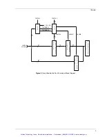
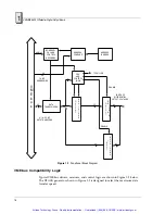
Страница 9: ... the user to test most of the circuitry on the board When the VMIVME 2533 is in test mode data which is written to the output registers can be read back to verify proper operation This can be done without driving the output cable and without disturbing the field circuitry connected to the VMIVME 2533 Figure 2 below shows a simplified diagram of the Built in Test features of the VMIVME 2533 Figure ...

Страница 10: ...EST MODE 1 TEST MODE 2 P A L CONTROL 9 3 4 CONTROL ENABLE ENABLE O U T P U T R E G I S T E R S 32 32 BITS OF DATA 32 C A B L E D R I V E R S 32 64 C A B L E R E C E I V E R S O U T P U T C O N N E C T O R Artisan Technology Group Quality Instrumentation Guaranteed 888 88 SOURCE www artisantg com ...

Страница 11: ... output voltage drivers to the field connector The Control and Status Register CSR contains three bits One bit controls the on board Fail LED while the other two bits along with some additional logic control the test functions of the board Built in Test logic enables the output data to be read back without affecting the signals to the field System reset puts the board into test mode for immediate ...

Страница 12: ...lication and Configuration Guides are available from GE to assist the user in the selection specification and implementation of systems based on GE s products Title Document No Digital Input Board Application Guide 825 000000 000 Low Level Analog I O Configuration Guide 825 000000 001 Change of State Application Guide 825 000000 002 Digital I O with Built in Test Product Line Description 825 00000...

Страница 13: ... hazard Keep Away from Live Circuits Operating personnel must not remove product covers Component replacement and internal adjustments must be made by qualified maintenance personnel Do not replace components with power cable connected Under certain conditions dangerous voltages may exist even with the power cable removed To avoid injuries always disconnect power and discharge circuits before touc...

Страница 14: ...re a practice a condition which if not correctly performed or adhered to could result in injury or death to personnel CAUTION This sign denotes a hazard It calls attention to an operating procedure a practice or a condition which if not correctly performed or adhered to could result in damage to or destruction of part or all of the system NOTE Calls attention to a procedure a practice a condition ...

Страница 15: ... Overview 15 Built In Test Description 21 Introduction This section of the manual presents detailed information concerning the hardware operation of the board 1 Artisan Technology Group Quality Instrumentation Guaranteed 888 88 SOURCE www artisantg com ...

Страница 16: ...w These sections are described in more detail in the following sections To perform an output data transfer data is written into Output Data Registers ODRs which latch the data The latched data is used by the output driver stage of the board Artisan Technology Group Quality Instrumentation Guaranteed 888 88 SOURCE www artisantg com ...

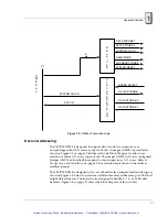
Страница 17: ...ximum data transfer speed BOARD SEL PAL AND CONTROL RECEIVERS ADDRESS COMPARE ADDRESS JUMPERS 8 16 32 BIT DATA TRANSFERS 32 13 3 R E G I S T E R S O U T P U T D R I V E R S 32 32 64 16 BIT ADDRESSING V M E b u s DATA TRANSCEIVERS CSR AND CONTROL LOGIC TO FAIL LED O U T P U T 32 BITS OF DIFFERENTIAL OUTPUT VOLTAGES ENABLE R E C E I V E R S I N P U T 32 64 ENABLE AM0 to 5 Artisan Technology Group Qu...

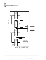
Страница 18: ... on page 22 for a detailed explanation of the address modifier jumper The VMIVME 2533 is designed with a set of board select jumpers and decode logic as shown in Figure 1 3 below to provide an efficient memory address map for CSR and output data addresses The board is also designed to handle 8 16 or 32 bit data transfers Figure 1 4 on page 19 shows the block diagram of this circuitry P1 R E C E I ...

Страница 19: ...R BOTH C O M P A R A T O R C O M P A R A T O R J U M P E R S 8 A D D R E S S A D D R E S S J U M P E R S V M E b u s P1 D A T A C S R C O M P A R A T O R A D D R E S S J U M P E R S A D D R E S S J U M P E R S P A L CSR SELECT DATA SELECT AM2 A2 to A7 A1 to A7 AM2 8 7 D A T A C S R AM2 JUMPER AM2 JUMPER Artisan Technology Group Quality Instrumentation Guaranteed 888 88 SOURCE www artisantg com ...

Страница 20: ...5 IDB00 to IDB07 IDB16 to IDB23 P1 V M E b u s D00 to D07 D08 to D15 T R A N S C E I V E R T R A N S C E I V E R IDB08 to IDB15 IDB24 to IDB31 T R A N S C E I V E R 8 8 HI WORD DTA BUS EN L D16 to D23 8 P2 D24 to D31 8 V M E b u s WRITE L LO WORD DATA BUS EN L SEL HI WORD ONLY L Artisan Technology Group Quality Instrumentation Guaranteed 888 88 SOURCE www artisantg com ...

Страница 21: ...ED is illuminated The CSR uses only the upper nibble bits 7 through 4 for controlling the test mode functions The lower nibble bits 3 through 0 can be setup by the user via jumper JA These bits can define some function for the user to test in software The CSR also contains a board ID code register on the upper byte Its value is 02 HEX This register can be used by system software to do automatic sy...

Страница 22: ...hipped Upon system reset the CSR is cleared to all zeroes initializing the board in the off line test mode This mode of test disables all output drivers enables the output registers and internal loopback registers to test the board circuitry without affecting off board circuitry The on line test mode is the normal mode of operation for the VMIVME 2533 In this mode the VMIVME 2533 has a differentia...

Страница 23: ...ents Jumper Configuration 23 Address Modifiers 24 Data Registers Base Address 25 CSR Base Address 26 I O Cable and Front Panel Connector Configuration 27 2 Artisan Technology Group Quality Instrumentation Guaranteed 888 88 SOURCE www artisantg com ...

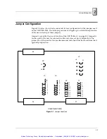
Страница 24: ...use of four bits of the CSR Table 3 1 on page 33 Jumper JA can be used by the user for automatic software system set up configuration The jumper JB is to be used for future enhancements and should not be moved from the G ground pin position Figure 2 1 Jumper Locations P1 P2 8 G 9 10 11 12 13 14 8 9 10 11 12 13 14 2 3 4 5 6 7 P3 5 JD JA JF JE C B A 2 3 4 5 6 7 C B A 1 JC 5 G JB 15 15 Artisan Techno...

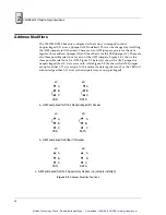
Страница 25: ...ee possible selections for AM2 Figure 2 2 below a shows the AM2 jumper for nonprivileged short I O accesses only while Figure 2 2 b shows the AM2 jumper set up for either I O access type In this mode the data registers and or the CSR will acknowledge either I O access short supervisory or non privileged Figure 2 2 Address Modifier Positions JC JD A B C A B C CSR DATA a AM2 Jumpered for Short Nonpr...

Страница 26: ...tory sets up these headers to a base address of 0000 HEX as shown in Figure 2 3 below Figure 2 3 Data Registers Base Address Configuration JD JF A B C 2 3 4 5 6 7 8 9 10 11 12 13 14 15 ADDRESS BIT 08 ADDRESS BIT 15 ADDRESS BIT 02 ADDRESS BIT 07 ADDRESS MODIFIER SELECTION JUMPERS See Figure 5 4 1 JUMPER INSTALLED 0 OPEN 1 Artisan Technology Group Quality Instrumentation Guaranteed 888 88 SOURCE www...

Страница 27: ...tem can be stacked into separate but contiguous memory locations The CSR jumpers JC and JE are configured at the factory to a base address of 0004 HEX as shown in Figure 2 4 below Figure 2 4 CSR Base Address Configuration JC JE A B C 1 2 3 4 5 6 8 9 10 11 12 13 14 15 ADDRESS BIT 08 ADDRESS BIT 15 ADDRESS BIT 01 ADDRESS BIT 07 JUMPER INSTALLED 0 OPEN 1 7 ADDRESS MODIFIER SEE FIGURE 5 4 1 Artisan Te...

Страница 28: ...er 1 shown at the bottom of the connector as it plugs into the header due to pin number 1 of P3 being mounted as shown Connector pin assignments for the 32 output channels of the VMIVME 2533 are shown in Table 2 1 on page 29 The VMIVME 2533 is a differential output board and so Pin A of each row is the output high side and Pin C of each row is the low side of the assigned channel The output connec...

Страница 29: ...N 29 PIN 28 PIN 27 PIN 26 PIN 25 PIN 24 PIN 23 PIN 22 PIN 21 PIN 20 PIN 19 PIN 18 PIN 17 PIN 16 PIN 15 PIN 14 PIN 13 PIN 12 PIN 11 PIN 10 PIN 9 PIN 8 PIN 7 PIN 6 PIN 5 PIN 4 PIN 3 PIN 2 PIN 1 FRONT VIEW OF P3 CONNECTOR A C Artisan Technology Group Quality Instrumentation Guaranteed 888 88 SOURCE www artisantg com ...

Страница 30: ...2 31 30 29 28 27 26 25 24 23 22 21 20 19 18 17 16 15 14 13 12 11 10 09 08 07 06 05 04 03 02 01 31 30 29 28 27 26 25 24 23 22 21 20 19 18 17 16 15 14 13 12 11 10 09 08 07 06 05 04 03 02 01 00 P3 Output Connector Channel Assignments Artisan Technology Group Quality Instrumentation Guaranteed 888 88 SOURCE www artisantg com ...

Страница 31: ...N 3 PIN 4 PIN 5 PIN 6 PIN 7 PIN 8 PIN 9 PIN 10 PIN 11 PIN 12 PIN 13 PIN 14 PIN 15 PIN 16 PIN 17 PIN 18 PIN 19 PIN 20 PIN 21 PIN 22 PIN 23 PIN 24 PIN 25 PIN 26 PIN 27 PIN 28 PIN 29 PIN 30 PIN 31 C B A PIN 32 P C BOARD Artisan Technology Group Quality Instrumentation Guaranteed 888 88 SOURCE www artisantg com ...

Страница 32: ... are mapped into the same address locations as the drivers Therefore the bits of each register correspond to an output channel when performing a write to that register but the output data can be read back by performing a read cycle The base address required for accessing the VMIVME 2533 is selected by the address jumpers JD and JF referred to Chapter 2 Configuration and Installation on page 22 The...

Страница 33: ...ess that causes selection of the board When the CPU executes an instruction to store data VMEbus control signals cause the board to store the output data as transferred from the VMEbus The format of the output data and the board address is shown in Table 3 1 on page 33 Artisan Technology Group Quality Instrumentation Guaranteed 888 88 SOURCE www artisantg com ...

Страница 34: ...9 IDB 8 IDB 7 IDB 6 IDB 5 IDB 4 IDB 3 IDB 2 IDB 1 IDB 0 I O 15 I O 14 I O 13 I O 12 I O 11 I O 10 I O 9 I O 8 I O 7 I O 6 I O 5 I O 4 I O 3 I O 2 I O 1 I O 0 0 Y Y Y 1 IDB 7 IDB 6 IDB 5 IDB 4 IDB 3 IDB 2 IDB 1 IDB 0 Y Y X Y X X X DATA PORT 0 UPPER BYTE DATA PORT 1 MIDDLE UPPER BYTE DATA PORT 2 MIDDLE LOWER BYTE DATA PORT 3 LOWER BYTE I O 31 I O 30 I O 29 I O 28 I O 27 I O 26 I O 25 I O 24 CONTROL ...

Страница 35: ...vers These outputs can be read by differential line receivers for on line Built in Test when TM1 is high The CSR address is selected by the address jumpers JC and JE The format of the CSR data and address is shown in Table 3 1 on page 33 The CSR is initialized active upon system reset such that the outputs are disabled and the front panel LED is illuminated Jumper JA can be used by the user for so...

Страница 36: ...mov ing the board from the chassis 8 Quality of cables and I O connections If products must be returned contact GE for a Return Material Authorization RMA Number This RMA Number must be obtained prior to any return from Customer Care GE Customer Care is available at 1 800 433 2682 in North America or 1 780 401 7700 for international calls Or visit our website at www ge ip com Maintenance Prints Us...

Страница 37: ...TIONS OR WARRANTIES OF ANY KIND WHETHER EXPRESS OR IMPLIED INCLUDING BUT NOT LIMITED TO WARRANTIES OF DESIGN MERCHANTABILITY OR FITNESS FOR A PARTICULAR PURPOSE ALL OTHER LIABILITY ARISING FROM RELIANCE UPON ANY INFORMATION CONTAINED HEREIN IS EXPRESSLY DISCLAIMED GE Intelligent Platforms Information Centers Americas 1 800 322 3616 or 1 256 880 0444 Asia Pacific 86 10 6561 1561 Europe Middle East ...

Страница 38: ...l service in house repair center WE BUY USED EQUIPMENT Sell your excess underutilized and idle used equipment We also offer credit for buy backs and trade ins www artisantg com WeBuyEquipment REMOTE INSPECTION Remotely inspect equipment before purchasing with our interactive website at www instraview com LOOKING FOR MORE INFORMATION Visit us on the web at www artisantg com for more information on ...

Отзывы: