17
Operational Overview
1
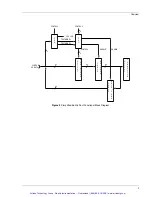
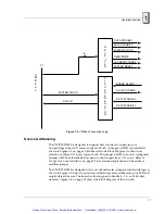
Figure 1-2
VMEbus Foundation Logic
Device Addressing
The VMIVME-2533 is designed to support data transfers in supervisory or
non-privileged short I/O memory space or both. A jumper (AM02) is provided as
shown in Figure 1-3 on page 18 (Address Decode Block Diagram) to allow user
selection of either I/O access type or both. The jumper (AM02) is factory configured
(jumper AM02 not installed) to respond to short supervisory I/O access. Refer to
Configuration and Installation
on page 22 for a detailed explanation of the address
modifier jumper.
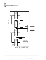
The VMIVME-2533 is designed with a set of board select jumpers and decode logic as
shown in Figure 1-3 below to provide an efficient memory address map for CSR and
output data addresses. The board is also designed to handle 8-, 16-, or 32-bit data
transfers. Figure 1-4 on page 19 shows the block diagram of this circuitry.
P1
R
E
C
E
I
V
E
R
D
T
A
C
K
G
E
N
E
R
A
T
O
R
6
SYSTEM CLOCK
BOARD SELECT
DATA STROBE 1
DATA STROBE 2
READ/WRITE
ADDRESS STROBE
SYSTEM RESET
DELAY STROBE
DATA STROBE 0
DATA STROBE 1
DTACK*
V
M
E
b
u
s
SYSTEM CLOCK
Artisan Technology Group - Quality Instrumentation ... Guaranteed | (888) 88-SOURCE | www.artisantg.com


