background image

© 2011 GE Intelligent Platforms Embedded 

Systems, Inc. All rights reserved.

All trademarks are the property of their 

respective owners.

Confidential Information - This document 

contains Confidential/Proprietary Information 

of GE Intelligent Platforms, Inc. and/or its 

suppliers or vendors.  Distribution or 

reproduction prohibited without permission.

THIS DOCUMENT AND ITS CONTENTS ARE 

PROVIDED "AS IS", WITH NO REPRESENTATIONS 

OR WARRANTIES OF ANY KIND, WHETHER 

EXPRESS OR IMPLIED, INCLUDING BUT NOT 

LIMITED TO WARRANTIES OF DESIGN, 

MERCHANTABILITY, OR FITNESS FOR A 

PARTICULAR PURPOSE.  ALL OTHER LIABILITY 

ARISING FROM RELIANCE UPON ANY 

INFORMATION CONTAINED HEREIN IS 

EXPRESSLY DISCLAIMED.

GE Intelligent Platforms 
Information Centers

Americas:

1 800 322 3616 or 1 256 880 0444

Asia Pacific:

86 10 6561 1561

Europe, Middle East and Africa:

Germany

+49 821 5034-0

UK

+44 1327 359444

Additional Resources

For more information, please visit
the GE Intelligent Platforms Embedded 
Systems web site at:

www.ge-ip.com

Publication No. IPN250RTM-HRM/2

Содержание IPN250RTM

Страница 1: ...Hardware Reference Manual IPN250RTM Edition 2 Publication No IPN250RTM HRM 2 GE Intelligent Platforms ...

Страница 2: ...rdance with the requirements of the WEEE Directive GE Intelligent Platforms Limited will evaluate requests to take back products purchased by our customers before August 13 2005 on a case by case basis A WEEE management fee may apply Edition Date Description 1 June 2010 Board Artwork Rev 1 1 errata January 2011 Errata to Fig 1 3 and Section 2 3 7 1 errata February 2011 Errata to Section 2 1 and Ta...

Страница 3: ...areas when K M and G mean 210 220 and 230 respectively NOTE When describing transfer rates k M and G mean 103 106 and 109 not 210 220 and 230 Multiple bit fields are numbered from 0 to n where 0 is the LSB and n is the MSB Text Signal names ending with a tilde denote active low signals all other signals are active high Notices This guide uses the following types of notice NOTE Notes call attention...

Страница 4: ...BRTMP1 HRM LINK SCVPX6U Hardware Reference Manual publication number SCVPX6U HRM LINK VPX I O Modules Hardware Reference Manual publication number VPXIOM 0HH GE Websites Information regarding all GE Intelligent Platforms products can be found on the following website LINK http www ge ip com products family embedded systems Third Party Manuals ANSI VITA 46 0 2007 VPX Baseline Standard VITA 65 OpenV...

Страница 5: ...quest SR number for use in future correspondence Alternatively you may also contact GE Intelligent Platformsʹ Technical Support via LINK support towcester ip ge com TELEPHONE 44 0 1327 322760 Returns If you need to return a product there is a Return Materials Authorization RMA request form that can be printed out and filled in available via the web site Repairs page LINK http www ge ip com support...

Страница 6: ...nector J10 18 2 3 5 GPIO Header P1 18 2 3 6 JTAG Header P2 18 2 3 7 Spare Signals Header P3 19 2 3 8 P3V3 Header P4 19 2 3 9 Dediprog Interface Header P5 19 2 3 10 SATA0 1 Connectors P9 P10 20 2 4 IPN250RTMB 21 2 4 1 HDMI Connector J2 21 2 4 2 TV Capture Connectors J3 to J6 21 2 4 3 Multi Display Connector J7 22 2 4 4 GPU DVI Dual Link Connector J8 23 2 4 5 USB0 1 Connectors J10 J9 23 2 4 6 USB2 3...

Страница 7: ...Publication No IPN250RTM HRM 2 Table of Contents 7 3 2 2 PCIe Switch configuration LEDs DS27 to DS33 28 3 2 3 Power Good LED DS34 29 ...

Страница 8: ...ide the fabric connections wired into the backplane The OVPX64UBP backplane functionality is described in the SCVPX6U development chassis manual LINK SCVPX6U Hardware Reference Manual publication number SCVPX6U HRM 1 2 Fitting RTMs See the VPX I O Modules manual for fitting instructions LINK VPX I O Modules Hardware Reference Manual publication number VPXIOM 0HH 1 3 Current Requirements The IPN250...

Страница 9: ...ks connectors switches headers and LEDs described in this document Figure 1 3 shows the combined IPN250RTMA and IPN250RTMB assembly with a monolithic 1 6 inch front panel NOTE The assembly will not fit within the height profile of a single VPX backplane slot and will encroach into the area normally reserved for the RTM of the adjacent slot TIP If the 1 6 inch pitch IPN250RTM 111 assembly does not ...

Страница 10: ...10 IPN250RTM Publication No IPN250RTM HRM 2 Figure 1 2 IPN250RTMB ...

Страница 11: ...Publication No IPN250RTM HRM 2 IPN250RTM 11 Figure 1 3 IPN250RTMA and IPN250RTMB Assembly ...

Страница 12: ...t Profile with the following non fabric connectivity P0 J0 is used by the Utility plane P3 J3 is user defined P4 J4 is partly used by the Control planes The remainder of P4 J4 and the single ended signals are all user defined A Control plane of two ultra thin pipes A Control plane of two thin pipes P5 J5 is user defined P6 J6 is user defined ...

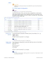
Страница 13: ...eT Ethernet CPUTP1 J5 1000Base KX Ethernet CPUTP2 J4 1000Base KX Ethernet CVBS 2 J3 TV capture DLDVI 1 J8 GPU DVI Dual link HDMI J2 HDMI interface PCIe1 J6 PCIe Interface PCIe2 J7 PCIe Interface SATA 0 P9 SATA interface SATA 1 P10 SATA interface USB 0 J10 USB interface USB 1 J9 USB interface USB 2 J11 USB interface USB 3 J12 USB interface x IPN250RTMA J10 IPN250RTM interface x IPN250RTMA P1 GPIO h...

Страница 14: ...he active connector and the GPU 2 3 IPN250RTMA 2 3 1 1000BaseT Ethernet Channel 1 2 Connector J3 The IPN250RTM supports two thin pipes on the Control Plane as defined by the OpenVPX Payload Slot Profile SLT6 PAY 4F1Q2UT2T 10 2 1 These pipes are brought out to a dual side by side RJ45 type connector pinned out to the TIA EIA 568 standard The signal pairs are 100 differential and matched GEIP offers...

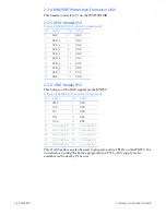
Страница 15: ...s two ports of 1 lane PCIe on the IPN250RTM NOTE The PCIe differential pairs can only be used as two 1 lane ports they cannot be used together to form a single 2 lane PCIe port J6 and J7 provide the PCIe interfaces via two Molex 75586 0007 PCI Express Cabling Standard 8 lane PCIe cable connectors On both connectors only the first lane is populated the other lanes have their positive negative pairs...

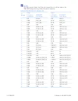
Страница 16: ...k to B12 PETP3 100R link to A12 12 PERN3 100R link to B11 PETN3 100R link to A11 13 GND GND GND GND 14 PWR P3V3_AUX CREFCLKP 100R link to A15 15 PWR P3V3_AUX CREFCLKN 100R link to A14 16 PWR P3V3_AUX GND GND 17 PWR_RTN GND RSVD NC 18 PWR_RTN GND RSVD NC 19 PWR_RTN GND SB_RET 10kR link to P3V3_AUX 20 CWAKE 10kR link to P3V3_AUX CPRSNT 10kR link to P3V3_AUX 21 CPERST 10kR link to P3V3_AUX CPWRON 10k...

Страница 17: ...12 12 PERN3 100R link to B11 PETN3 100R link to A11 13 GND GND GND GND 14 PWR P3V3_AUX CREFCLKP 100R link to A15 15 PWR P3V3_AUX CREFCLKN 100R link to A14 16 PWR P3V3_AUX GND GND 17 PWR_RTN GND RSVD NC 18 PWR_RTN GND RSVD NC 19 PWR_RTN GND SB_RET 10kR link to P3V3_AUX 20 CWAKE 10kR link to P3V3_AUX CPRSNT 10kR link to P3V3_AUX 21 CPERST 10kR link to P3V3_AUX CPWRON 10kR link to P3V3_AUX 22 GND GND...

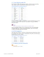
Страница 18: ...upply is also available on the nearby P4 header Table 2 6 IPN250RTMA P1 Header Pin Assignments Pin Signal Pin Signal 1 GND 2 GND 3 GPIO_0 4 GND 5 GPIO_1 6 GND 7 GPIO_2 8 GND 9 GPIO_3 10 GND 11 GPIO_4 12 GND 13 GPIO_5 14 GND 15 GPIO_6 16 GND 17 GPIO_7 18 GND 19 GND 20 GND Table 2 7 IPN250RTMA P2 Header Pin Assignments Pin Signal Pin Signal 1 TRST 2 GND 3 TDO 4 GND 5 TDI 6 GND 7 TMS 8 GND 9 TCLK 10 ...

Страница 19: ...SPAREx_TP pin on the header connects the SPAREx signal to the test point 2 3 8 P3V3 Header P4 This header is provided for convenience in using the Lattice programmer with the JTAG Header P2 All pins on P4 are connected to P3V3_AUX so that the Lattice programmer can use any of them 2 3 9 Dediprog Interface Header P5 CAUTION This header is now a no fit option Table 2 8 IPN250RTMA P3 Header Pin Assig...

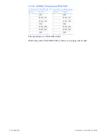
Страница 20: ... 100 differential GEIP offers cable C CBL000155 001 which is a 0 6m long SATA cable Table 2 10 IPN250RTMA P9 P10 Connector Pin Assignments P9 Pin Signal P10 Pin Signal 1 GND 1 GND 2 SATA0_TXP 2 SATA1_TXP 3 SATA0_TXN 3 SATA1_TXN 4 GND 4 GND 5 SATA0_RXN 5 SATA1_RXN 6 SATA0_RXP 6 SATA1_RXP 7 GND 7 GND ...

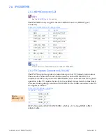
Страница 21: ... for testing basic operation of the TV capture device J4 to J6 are fitted in board and are most likely to be used during design validation of the IPN250 The SSMB connectors route the TV signals as follows GEIP offers cable ARACC 3BNCSSMB1 which is a 1 9m long SSMB to BNC adaptor cable Table 2 11 IPN250RTMB J2 Pin Assignments Pin Signal Pin Signal 1 GND 2 HDMI_DVI_TX2P 3 HDMI_DVI_TX2N 4 GND 5 HDMI_...

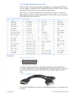
Страница 22: ...ly is required a suitable Multi Display to VGA adaptor can be used Table 2 13 IPN250RTMB J7 Pin Assignments Pin Signal Pin Signal Pin Signal Pin Signal 1 Quiet GND 30 DVI_TXD0N 31 DVI_CLKP 60 Quiet GND 2 VGA2_RED 29 DVI_TXD0P 32 DVI_CLKP 59 VGA2_GREEN 3 VGA2_BLUE 28 DVI_TXD1N 33 GND 58 Unconnected 4 Quiet GND 27 DVI_TXD1P 34 GND 57 GND 5 DVI_DDC_5V 26 DVI_TXD2N 35 GND 56 VGA2_HSYNC 6 DDC2_CLOCK_DV...

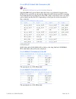
Страница 23: ... The signal pairs are 90 differential Table 2 14 IPN250RTMB J8 Pin Assignments Pin Signal Pin Signal Pin Signal Pin Signal 1 DVI_DL_TX2Nb 9 DVI_DL_TX1Nb 17 DVI_DL_TX0Nb A1 VGA1_GREEN 2 DVI_DL_TX2Pb 10 DVI_DL_TX1Pb 18 DVI_DL_TX0Pb A2 VGA1_REDa a Routed over Quiet GND 3 GND 11 GND 19 GND A3 VGA1_BLUEa 4 DVI_DL_TX4Nb 12 DVI_DL_TX3Nb 20 DVI_DL_TX5Nb A4 VGA1_HSYNC 5 DVI_DL_TX4Pb 13 DVI_DL_TX3Pb 21 DVI_...

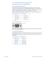
Страница 24: ...N250RTMB P3 Pin Numbering GEIP offers cable C CBL000099 001 which is a 2m long null modem serial cable with 9 way socket connectors 2 4 9 Audio Header P4 The IPN250 supports a stereo pair left and right of audio inputs and a stereo pair left and right of audio outputs Signal names input output are with respect to the IPN250 Table 2 2 IPN250RTMB P3 Pin Assignments Pin Signal Pin Signal 1 Interconne...

Страница 25: ... following table gives RS232 and RS422 485 versions of the available signals Table 2 4 IPN250RTMB P5 Pin Assignments Pin Signal Pin Signal 1 Interconnecta a Pins 1 7 and 8 are connected together 2 Unconnected 3 COM2_RXD_RXN 4 COM2_CTS_RXP 5 COM2_TXD_TXN 6 COM2_RTS_TXP 7 Interconnecta 8 Interconnecta 9 GND 10 Unconnected ...

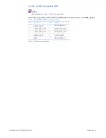
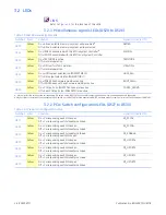
Страница 26: ...ayload boards being set as System Controller Whichever is not used should have DIP switches links set left open CAUTION A system should not contain more than one System Controller Table 3 1 IPN250RTMA P7 Switch Assignments P7 Switch Function Description Associated LED 1 COM12_FRONT Closed COM ports on IPN250 front panel are active Open Rear COM ports on IPN250RTM are active DS26 2 BOOT_FWH Leave o...

Страница 27: ...cted by the binary value set of switches 6 and 7 as follows 00b x16 01b x4 x4 x4 x4 10b x8 x4 x4 11b x8 x8 Where 0 switch closed and 1 switch open NOTE An inverter has been included on the bit 0 signal line to invert operation to that described for this bit in the PCIe switch data sheet Table 3 2 IPN250RTMA P8 Switch Assignments P8 Switch Function Description Associated LED 1 NT_UPORT0 Sets the No...

Страница 28: ... Off Rear COM ports on IPN250RTM are active COM12_FRONT a May not reflect the setting of the corresponding DIP switch on the IPN250RTM if non volatile memory has been write enabled elsewhere in the system b May not reflect the setting of the corresponding DIP switch on the IPN250RTM if the associated IPN250 has been made System Controller via the backplane or FABRTMP1 Table 3 4 PCIe Switch Configu...

Страница 29: ...tween the HDMI and DVI outputs on the IPN250RTM requires a local 3 3V supply An on board regulator produces this voltage from the P5V supply This red power good LED shows when this power supply is operational CAUTION Do not assume that this LED shows that the power supply is within a specific voltage tolerance ...

Страница 30: ...TIONS OR WARRANTIES OF ANY KIND WHETHER EXPRESS OR IMPLIED INCLUDING BUT NOT LIMITED TO WARRANTIES OF DESIGN MERCHANTABILITY OR FITNESS FOR A PARTICULAR PURPOSE ALL OTHER LIABILITY ARISING FROM RELIANCE UPON ANY INFORMATION CONTAINED HEREIN IS EXPRESSLY DISCLAIMED GE Intelligent Platforms Information Centers Americas 1 800 322 3616 or 1 256 880 0444 Asia Pacific 86 10 6561 1561 Europe Middle East ...

Отзывы: